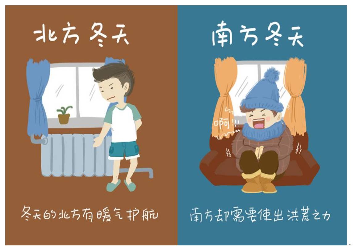
The northwest wind is howling, and the annual heating season has arrived. Heating pipelines are so important during the winter in the north. The design of the pipelines is aimed at maximizing effective thermal energy under determined energy conditions. Low power design aims to meet functional requirements with minimal power consumption. The low power design of chips is to ensure that the chip consumes the least energy while completing the required functions. It seems that one maximizes power consumption while the other minimizes it, two seemingly opposite tasks can actually be achieved using the same methods to obtain different results.
Low Power Design Methods (Pipeline Renovation Methods)
Pipeline renovation aims to ensure that every functional area in the house has warm heating. Under unified heating conditions, the utilization rate of heating is maximized, and under self-heating conditions, the least gas is consumed for the same bodily feeling. Low power design aims to minimize power consumption while completing chip functions.
The low power design of chips starts with a thorough understanding of the causes of chip power consumption. Based on the current power consumption situation, methods to reduce power consumption are sought from every aspect of architecture design, functional design, and physical implementation.
1. Clock tree optimization: Increase clock gating
2. Design adjustments: Reducing dynamic power can be achieved by increasing operational isolation, logic restructuring, logic reduction, inserting buffers, swapping pins, etc.
3. Multi-voltage domain libraries: Multi-voltage domain libraries can comprehensively consider design performance requirements while reducing dynamic power during design implementation.
4. Adjust design voltage: Use multi-supply voltage design, dynamic voltage and frequency scaling, and adaptive voltage and frequency scaling to optimize design.
5. Power shutdown: By adding power switches, power consumption can be effectively reduced.
6. Control substrate bias: Increase substrate bias to improve Vt and reduce leakage current, which will be applicable for 45nm and below processes.
7. Use transistors of different lengths: Long transistors will be slower than ordinary transistors by 10%, but can reduce static power consumption by 3 times.
8. Architecture adjustments: Prefer parallel structures in architecture to reduce power consumption at the cost of area; split memory, breaking large memory blocks into multiple parts, selectively shutting down unused memory power sources.
With methods available, how to implement them is the most important. Next, I will briefly introduce the process of implementing low power design.
Layout Planning (Pipeline Planning)
To renovate the heating pipeline, the first step is to plan the layout of the pipelines in the house, determining which rooms share the same pipeline: kitchen, study, bedroom, and bathroom. The first step in low power design is the overall power domain division, determining which functional modules can be placed on the same power path, ensuring that when the chip power pins supply power, the voltage of each functional module meets the requirements, while also considering potential wiring issues. This determines the entire chip’s power planning. The goal of layout planning is to arrange the chip reasonably so that the layout and wiring process can be completed smoothly, minimizing iteration times; factors like power, timing, congestion, and area are all critical. The same design can have different layout plans, with the goal of finding the best balance in time and area.
Implementation Techniques (Pipeline Techniques)
Once the pipeline planning is complete, the next step is to choose methods that can be used during the actual renovation process. This includes deciding whether to use underfloor heating or radiators during the design phase, adding switches to the heating pipelines, and providing shutdown control for functional areas, as well as adding bypass functions.
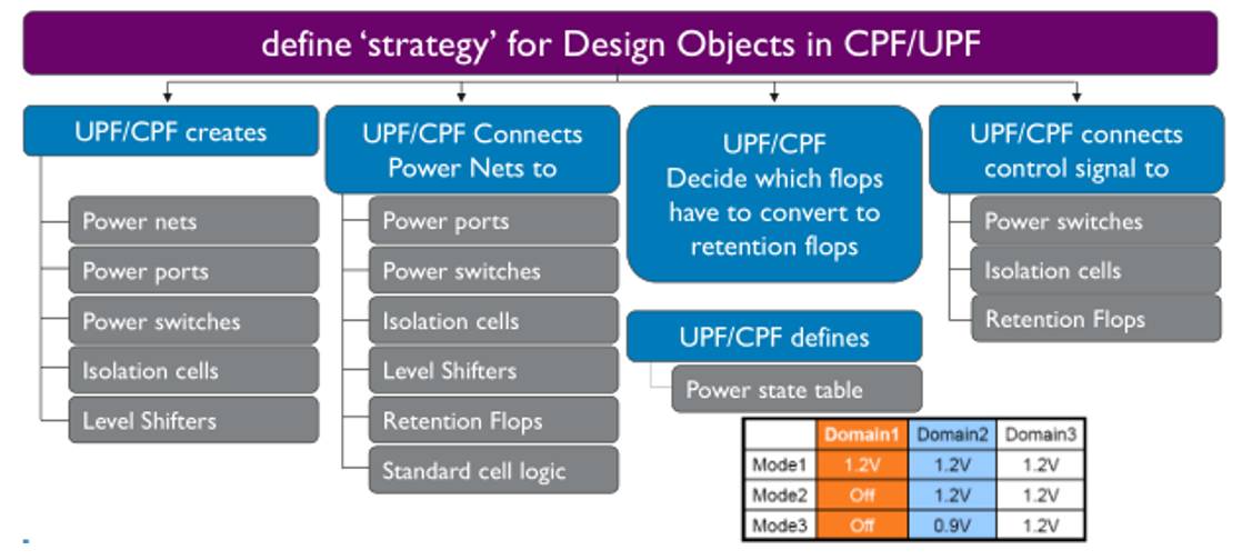
The current mainstream low power design process comprehensively considers the entire process from front-end RTL design, logic synthesis, to physical implementation, fulfilling overall power design requirements and reducing errors caused by different design stages, tools, and designers. Key optimization methods for low power design include area optimization, multi-voltage domains, gated clocks, multi-power domain design, and power shutdown. Currently, the industry uses CPF/UPF to complete the low power design process, mainly focusing on the following objectives during the design phase:
Low power design is reflected in every aspect of chip design implementation and will increase the workload of design, verification, and implementation. Using standardized low power design processes and methods is the only way to address this issue.
Library Selection (Heating Pipeline and Radiator Selection)
Choosing the right heating pipeline and radiator is a crucial step in heating renovation. Select the appropriate radiator based on the actual size of the room.
In the back-end design process, the physical implementation library needed is determined by application requirements. As shown in the figure below:
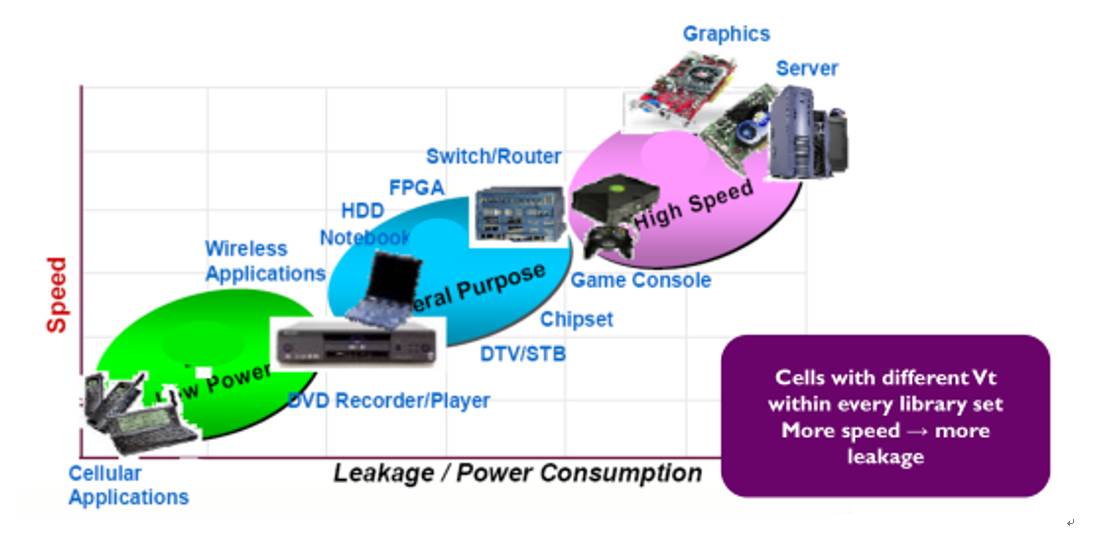
Based on actual application requirements, low power libraries can be selected, or general libraries or high-speed libraries, which will determine the choice of Core cell.
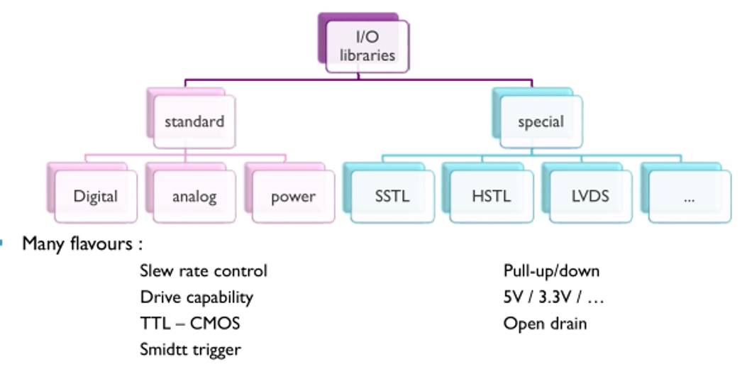
The choice of I/O mainly involves selecting standard libraries and special requirements, including the following types:
As processes increase, more and more libraries will be generated, and more boundary conditions and voltage selections will lead to more libraries, increasing the difficulty of selection. However, more precise libraries will make designs more consistent with actual production, which is also the ultimate goal of physical implementation.
Chip Layout and Wiring (Laying Heating Pipes)
With the pipeline planning completed and the radiators and pipes selected, the implementation of the heating pipeline can begin. Consider the shortest pipeline wiring, reduce unnecessary wiring, determine the placement of each pipeline switch, and complete the placement and connection of all pipelines. The layout and wiring of a chip is much more complex than laying heating pipes; after all, the number of lines in a chip far exceeds that of heating pipes, thus requiring more steps to ensure rationality and correctness, but the goal is the same: to complete the entire implementation.
The layout and wiring of a chip actually includes chip layout, clock tree synthesis, testable design, and chip wiring steps.
Traditional layout needs to consider area, wire length, and coverage, but now also timing, congestion, clock, and power consumption. Based on the design requirements, different design optimization methods can be used in timing-driven layouts, congestion-driven layouts, and power-driven layouts to ultimately achieve design goals. Establishing a clock tree is to solve the timing balance of all clock-related paths in the chip. For low power design, gated clocks and multi-clock domain designs have mature solutions to assist in completing designs and performing relevant basic rule checks. After establishing the basic clock tree, optimization is needed, including adjustments to buffer sizes, gate positions, and inserting delays, ultimately achieving design goals. Due to manufacturing or testing issues, chip failure problems are a significant challenge in current chip production. Increasing testable design can help identify issues earlier and reduce unnecessary subsequent processes and costs. Completing the above steps constitutes the chip wiring process, including global signal wiring, followed by signal wiring, and finally completing optimization based on results.
Multi-Mode Multi-Boundary Testing (Heating Shutdown Testing)
After deploying many switches in the heating pipeline, try to ensure that each radiator in every room can be shut down without affecting the heating of other rooms under different conditions, ensuring that every scenario meets design requirements.
In low power design, the same concept applies to multi-mode multi-boundary testing. With the addition of various low power-related technologies and multiple application scenarios, the original single-mode testing cannot meet practical needs. By establishing detailed testing scenarios, generating netlists and parameters under different modes, and completing timing analysis for all scenarios.
Of course, the backend process of the chip includes a series of complex processes, including on-chip verification, design finalization, tape-out packaging, and finally reaching the chip manufacturer to complete the tape-out work.
The heating pipeline has been laid out. In the upcoming heating season, one can spend the cold winter in the north in a warm environment. While you shiver in the warm winter in the south, I am warm as spring in the cold winter of the north.