With the official release of the first RISC-V Chinese book “Hands-On CPU Design – RISC-V Processor Edition” more and more enthusiasts are starting to use the open-source Hummingbird E203 RISC-V core, and many beginners have left messages asking about the use of the RISC-V toolchain.
To facilitate beginners in quickly learning RISC-V CPU design and RISC-V embedded development, the Hummingbird E203 open-source MCU prototype SoC (referred to as “MCU SoC” or “SoC” in this article) has customized a dedicated development board based on Xilinx FPGA (referred to as “FPGA Development Board” in this article) and a dedicated JTAG debugger (referred to as “JTAG Debugger” in this article).
This article will provide a detailed explanation of the Hummingbird FPGA Development Board and the Hummingbird JTAG downloader, and more information can be found at the bottom of the page by clicking “Read the original text” for more content.
Table of Contents
1 Overview
2 Hummingbird FPGA Development Board
2.1 Overview of FPGA Development Board
2.2 Purchase Channels for FPGA Development Board
2.3 Hardware Specifications of FPGA Development Board
2.4 Circuit Schematic of FPGA Development Board
2.5 MCU Section of FPGA Development Board
2.6 General Functionality of FPGA Development Board
2.7 Burning Hummingbird E203 Project to FPGA Development Board
2.8 Software Development and Debugging Using FPGA Development Board
3 Hummingbird JTAG Debugger
3.1 Overview of JTAG Debugger
3.2 Purchase Channels for JTAG Debugger
3.3 Connecting JTAG Debugger to FPGA Development Board
3.4 Using JTAG Debugger for Software Download and Debugging
1 Overview
To facilitate beginners in quickly learning RISC-V CPU design and RISC-V embedded development, the Hummingbird E203 open-source MCU prototype SoC (referred to as “MCU SoC” or “SoC” in this article) has customized a dedicated development board based on Xilinx FPGA (referred to as “FPGA Development Board” in this article) and a dedicated JTAG debugger (referred to as “JTAG Debugger” in this article).
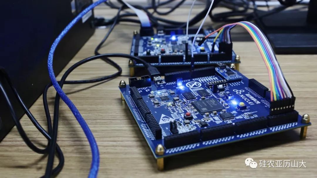
The complete FPGA development board prototype (including the FPGA development board and debugger) is shown in Figure 1-1.
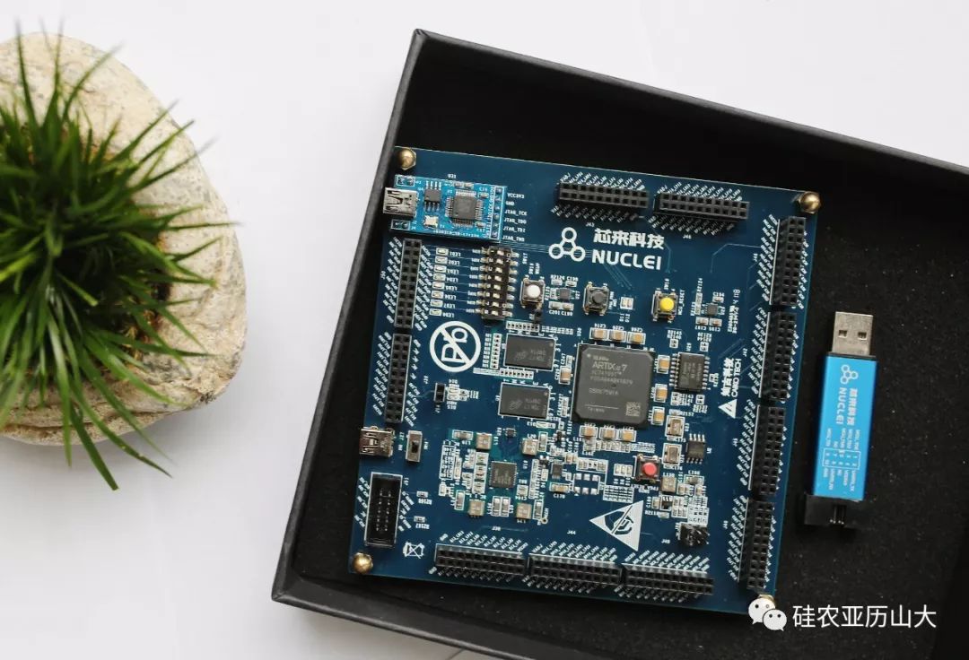
Figure 1-1 Hummingbird FPGA Development Board and JTAG Debugger, which will be detailed later.
2 Hummingbird FPGA Development Board Overview
2.1 Overview of FPGA Development Board
To facilitate the use of the Hummingbird FPGA development board, it has the following features:
Dual-use board, this development board can be used as a circuit design FPGA development board, and since it has pre-burned the Hummingbird E203 open-source SoC (including the E203 core), it can also serve directly as an MCU SoC prototype development board for embedded software development. That is:
(1) For users who do not understand FPGA software development, no operations are required; this development board comes pre-burned with the open-source Hummingbird E203 Core and the accompanying SoC, and can be used as an MCU embedded development board once powered on.
(2) For hardware users familiar with FPGA usage, it can also be treated as a standard FPGA development board to burn regular Verilog circuits for FPGA development.
Since the pre-burned Hummingbird E203 Core and the accompanying SoC source code are completely open-source, they can be modified or redeveloped at will.
Moreover, the open-source Hummingbird E203 MCU SoC’s “FPGA burning file (mcs format)” will be uploaded to:
https://github.com/SI-RISCV/e200_opensource/tree/master/fpga/nucleikit/prebuilt_mcs directory, allowing users to re-burn this FPGA board at any time to restore it to the pre-installed MCU embedded development board.
2.2 Purchase Channels for FPGA Development Board
Taobao purchase link for FPGA development board:
https://item.taobao.com/item.htm?id=580813056318
¥HoCVbR7Z0I3¥
(Copy this link and open it in the Taobao app to view)
2.3 Hardware Specifications of FPGA Development Board
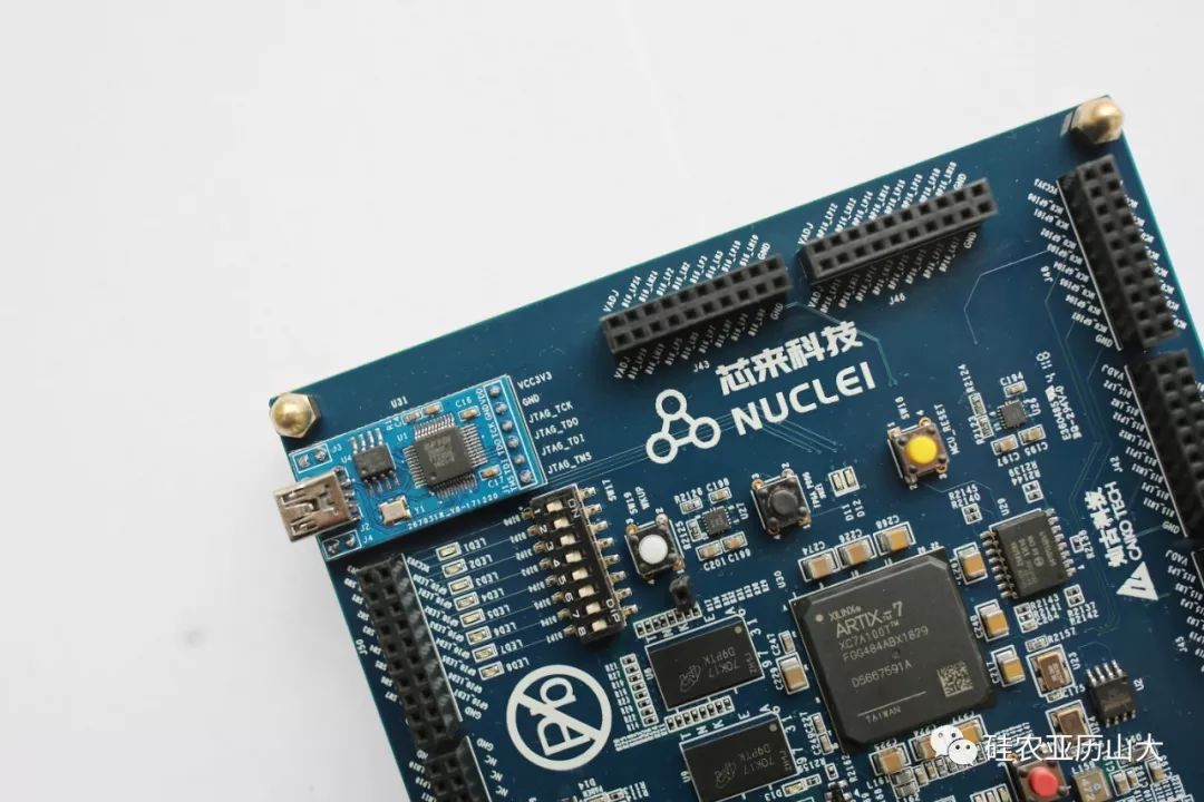
The Hummingbird E203 dedicated FPGA development board is an entry-level Xilinx FPGA development board, as shown in Figure 2-1.
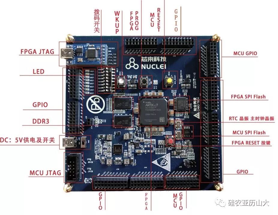
Figure 2-1 Overview of Hummingbird FPGA Development Board The hardware characteristics of this FPGA development board are as follows:
The FPGA model used is Xilinx XC7A100T.
Onboard dual crystal design: 100MHz main clock and 32.768K RTC clock.
Equipped with separate DC 5V power supply, and has a power switch, as marked in “DC: 5V power supply and switch” in Figure 2-1.
Equipped with an independent FPGA_RESET button, which can be used by the user as the reset button for the FPGA.
Equipped with up to 126 FPGA GPIOs for user-defined use.
Equipped with multiple power status indicator LED lights.
Equipped with an onboard Xilinx Platform Cable USB JTAG downloader for burning bitstreams to the FPGA, as marked in “FPGA JTAG” in Figure 2-1.
Equipped with two MT41K128M16JT-125K DDR III chips.
Equipped with a separate 128M-bit FPGA SPI Flash, which is used to store mcs format bitstream files:
(1) Users familiar with Vivado and Xilinx FPGA usage should know that once the bitstream file is burned into the FPGA, the FPGA cannot lose power; otherwise, the burned content will be lost, and it needs to be re-burned using Vivado’s Hardware Manager. To facilitate user usage, Xilinx FPGA development boards can write the contents to be burned into the Flash on the development board (in mcs format), and then automatically read the contents from the external Flash and burn them into the FPGA every time the FPGA is powered on (this process is very fast and does not affect user use). Since Flash is non-volatile memory, it retains its contents after power loss, meaning that once the contents are written to Flash, there is no need to manually re-burn using Hardware Manager after power loss (instead, the hardware circuit completes this quickly and automatically), allowing the FPGA to be used immediately upon power-up.
(2) In addition to automatically re-burning the FPGA upon power-up, users can also manually trigger the hardware circuit to use the contents in this Flash to re-burn the FPGA by pressing the “FPGA_PROG” button on the FPGA development board. The position of the “FPGA_PROG” button on the FPGA development board is indicated in Figure 2-1.
To facilitate the use of this development board directly as an MCU prototype embedded development board, the top-level pins of the Hummingbird E203 open-source SoC are directly connected to the development board, with clear silk screen markings. Please refer to section 2.5 for detailed introduction.
To facilitate this development board’s use as a standard FPGA development board, it is equipped with separate toggle switches and LED lights. Please refer to section 2.6 for detailed introduction.
2.4 Circuit Schematic of FPGA Development Board
The circuit schematic of this development board is stored at:
https://github.com/SI-RISCV/e200_opensource/tree/master/boards directory, please check it yourself.
(Viewing method: 1. Scroll to the end of the article and click “Read the original text” to view the total link of the e200_opensource project; 2. Reply “link” to the public account backstage to access)
2.5 MCU Section of FPGA Development Board
To facilitate this development board’s use directly as an MCU prototype embedded development board, the top-level pins of the “Hummingbird E203 open-source SoC” (referred to as SoC) are directly connected to the development board, with clear silk screen markings, as detailed in Figure 2-2, with the following key points:
The FPGA is pre-burned to become the “Hummingbird E203 open-source MCU SoC” (referred to as SoC)
To achieve MCU functionality, a Nor Flash is specially equipped on the FPGA development board for storing MCU software programs.
The two input clock inputs of the MCU SoC are generated as follows:
(1) The low-speed real-time clock is directly input from the 32.768KHz clock source on the FPGA development board (2) The high-speed clock is derived from the 100MHz clock on the FPGA development board, reduced in frequency to 16MHz via the internal PLL of the FPGA.
The relevant input and output pins of the SoC are clearly mapped to the FPGA development board and are clearly marked with printed font indicating the port numbers.
For detailed information on the input and output pin list of this SoC, please refer to the document “Introduction to Hummingbird E203 Open-source SoC” in the directory https://github.com/SI-RISCV/e200_opensource/blob/master/doc.
Note: All pins are only mapped to ordinary ports (bidirectional IO) inside the FPGA, and the FPGA Project maps these FPGA ports to these external predefined development board pins. For detailed information about the FPGA Project, please refer to the document “Quick Start Guide to Hummingbird E203” in the directory https://github.com/SIRISCV/e200_opensource/blob/master/doc.
More detailed descriptions are shown in Figure 2-2.
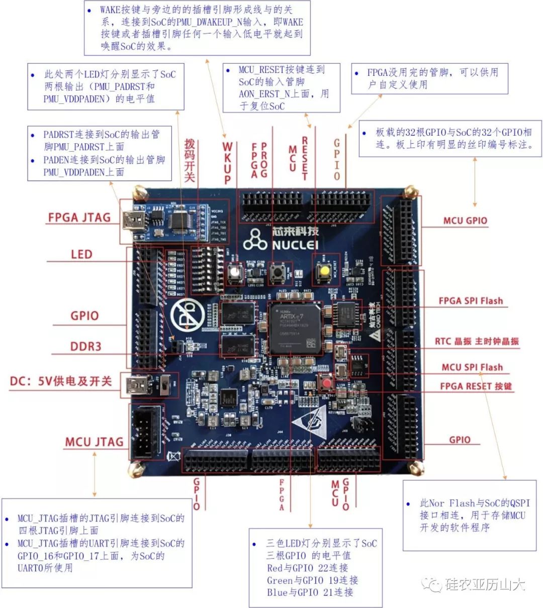
Figure 2-2 Custom MCU Section of Hummingbird FPGA Development Board
2.6 General Functionality of FPGA Development Board
To facilitate this development board’s use as a standard FPGA development board, it is equipped with separate toggle switches and LED lights, as shown in Figure 2-3.
Note: This set of toggle switches and LEDs is not connected to the FPGA pins, allowing users to freely jump wires to control other signals on the development board. As shown in Figure 2-3, users can connect the “toggle switch” to the MCU SoC’s GPIO interface using Dupont wires, effectively using the toggle switch to generate GPIO inputs, thus enabling programming to create simple visual demos.
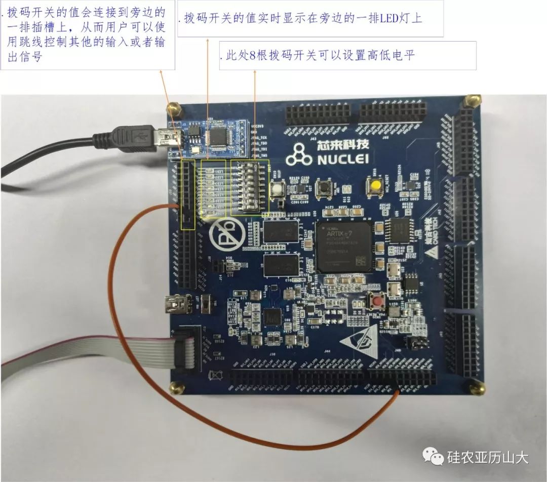
Figure 2-3 Toggle Switches and LED Lights of Hummingbird FPGA Development Board and Jumper Example
2.7 Burning Hummingbird E203 Project to FPGA Development Board
For specific operational steps on how to burn the Hummingbird E203 project (including SoC and processor core) to this FPGA development board, please refer to the document “Quick Start Guide to Hummingbird E203” in the directory https://github.com/SI-RISCV/e200_opensource/blob/master/doc.
2.8 Software Development and Debugging Using FPGA Development Board
For specific operational steps on how to use the FPGA development board for software development and debugging, please refer to the document “Quick Start Guide to Hummingbird E203” in the directory https://github.com/SI-RISCV/e200_opensource/blob/master/doc.
(Viewing method: 1. Scroll to the end of the article and click “Read the original text” to view the total link of the e200_opensource project; 2. Reply “link” to the public account backstage to access)
3 Hummingbird JTAG Debugger
3.1 Overview of JTAG Debugger
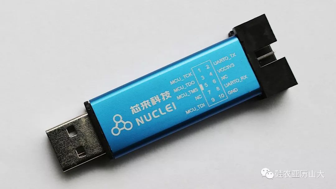
Figure 3-1 Dedicated JTAG Debugger for Hummingbird E203
To facilitate beginners in quickly learning RISC-V embedded development, the “Hummingbird MCU SoC” has customized a dedicated JTAG debugger that possesses the following characteristics:
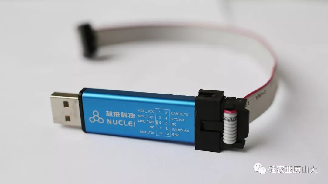
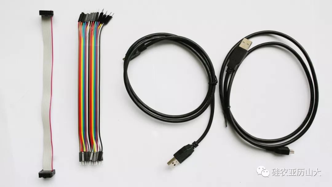
One end of the debugger is a standard USB interface, making it easy to plug directly into the USB port of the host PC, while the other end features a standard 4-wire JTAG interface and a 2-wire UART interface.
The debugger has USB-to-JTAG functionality and connects to the Hummingbird E203 FPGA development board via the standard 4-wire JTAG interface. Since the Hummingbird E203 core supports the standard JTAG interface, this interface can be used for program downloading or interactive debugging.
The debugger also has UART-to-USB functionality, connecting to the Hummingbird E203 FPGA development board via the standard 2-wire UART interface. Since embedded systems often lack displays, the UART port is commonly used to connect to the host PC’s COM port (or convert UART to USB and connect to the host PC’s USB port) for debugging, allowing the printf function in the embedded system to be redirected to the host’s display. Refer to Chapter 9 of the Chinese book “Introduction to RISC-V Architecture and Embedded Development” for more details.
3.2 Purchase Channels for JTAG Debugger
Taobao purchase link for FPGA development board:
https://item.taobao.com/item.htm?id=580813056318
¥HoCVbR7Z0I3¥
(Copy this link and open it in the Taobao app to view)
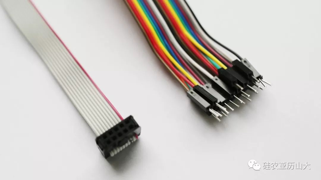
3.3 Connecting JTAG Debugger to FPGA Development Board
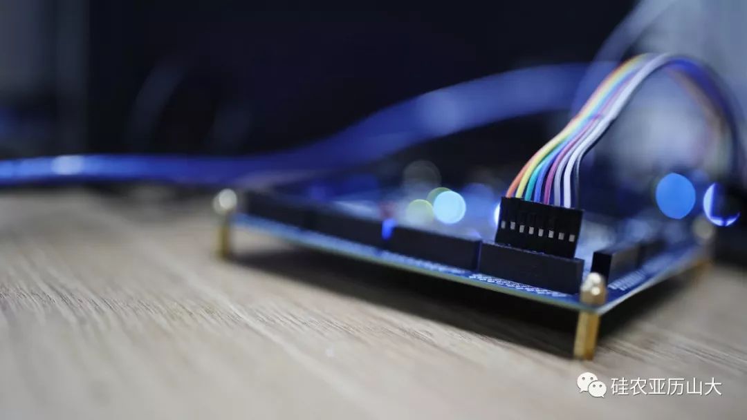
The connection method of the Hummingbird E203 JTAG debugger to the FPGA development board is shown in Figure 3-2.
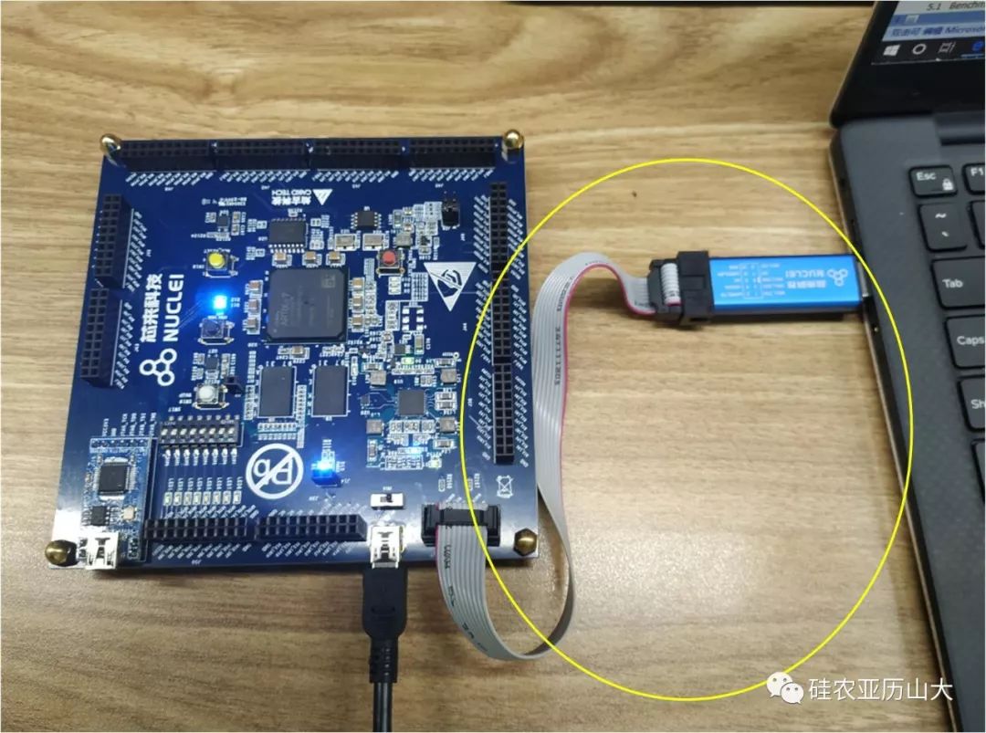
Figure 3-2 Connection of Hummingbird E203 Dedicated JTAG Debugger to PC and Development Board
3.4 Using JTAG Debugger for Software Download and Debugging
For specific operational steps on how to use the JTAG debugger for software download and debugging, please refer to the document “Quick Start Guide to Hummingbird E203” in the directory https://github.com/SI-RISCV/e200_opensource/blob/master/doc.
(Viewing method: 1. Scroll to the end of the article and click “Read the original text” to view the total link of the e200_opensource project; 2. Reply “link” to the public account backstage to access)
4 Purchase Links and Image Appreciation
Taobao purchase link for FPGA development board:
https://item.taobao.com/item.htm?id=580813056318
¥HoCVbR7Z0I3¥
(Copy this link and open it in the Taobao app to view)
Others
This article is edited by the new silicon farmer Pang Xia.
If you have any inquiries about this development board, please email [email protected]
More Information
Interested readers can follow the public account “Silicon Farmer Alexander” through the QR code below to learn more design tips and experience sharing related to Verilog, IC design, CPU, RISC-V, and artificial intelligence AI. Note: Due to the abundance of valuable content, please prepare tea.