On the 27th, reporters learned from Westlake University that Westlake Instrument (Hangzhou) Technology Co., Ltd., incubated by the university,has successfully developed an automated laser peeling technology for 12-inch silicon carbide substrates, solving the challenges of slicing ultra-large silicon carbide substrates of 12 inches and above.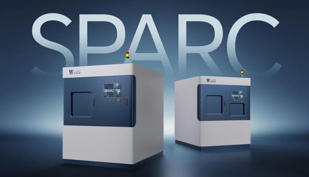 The laser peeling system for silicon carbide substrates. Image source: Westlake UniversityProfessor Qiu Min from the School of Engineering at Westlake University introduced that one of the important ways to reduce costs and increase efficiency in the silicon carbide industry is to manufacture larger-sized silicon carbide substrate materials. Compared to 6-inch and 8-inch substrates, the 12-inch silicon carbide substrate material expands the area available for chip manufacturing on a single wafer,which can significantly increase chip yield while reducing the unit manufacturing cost of chips under the same production conditions.