1. Introduction to W25Q128
W25Q128 is a 128M-bit (16MB) SPI interface Flash memory chip launched by Winbond, supporting standard SPI, Dual-SPI, and Quad-SPI modes. Key features include:
- Operating Voltage: 2.7V~3.6V
- Page Structure: 256 pages/block, 16KB per block, total of 1024 blocks
- Supports page programming (256 bytes/page)
- Erase operations supported: sector erase (4KB), block erase (32/64KB), full chip erase
- Maximum clock frequency of 104MHz
- Over 100,000 erase/write cycles
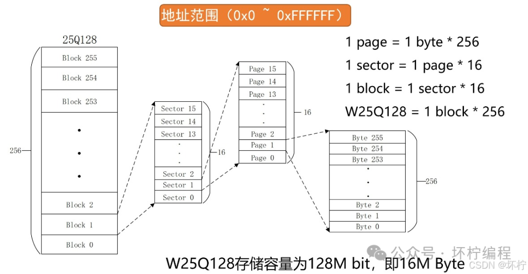
1.1 W25Q128 Storage Architecture
The W25Q128 memory adopts a hierarchical storage architecture, with a total capacity of 16MB (128Mbit). Its physical storage structure is divided as follows:
- Top-level division: 256 storage blocks (Block), each with a capacity of 64KB
- Block structure: each storage block contains 16 sectors (Sector), each sector with a capacity of 4KB
- Sector composition: each sector is subdivided into 16 storage pages (Page), each page with a capacity of 256 bytes
The erase mechanism of this memory has the following characteristics:
- The minimum erase unit is a single sector (4KB)
- When performing an erase operation, the entire sector must be processed
- The system must pre-allocate a 4KB aligned buffer to meet the physical erase granularity requirements
1.2 Common Commands for W25Q128
The W25Q128 has many commands; we will introduce a few commonly used ones.
| Command | (HEX) | Function |
|---|---|---|
| 0x06 | Write Enable | This command must be sent before writing data/erasing |
| 0x05 | Read SR1 | Determine if FLASH is in idle state, used for erasing |
| 0x03 | Read Data | Read data |
| 0x02 | Page Write | Write data, up to 256 bytes |
| 0x20 | Sector Erase | Sector erase command, minimum erase unit |
1.3 Detailed Operation Timing of W25Q128
- Write Enable (06h) – Command Function: Necessary enable signal for executing programming/erasing operations
- Operation Process:① CS pin set low (communication start)② Send 1 byte command code 06h (MSB first)③ CS pin set high (communication end)
- Status Impact: WEL bit (SR1) set to 1, valid for about 50ms
- Read Status Register (05h)
- Command Format:┌──────┬─────────────┐| Command Code | Response Data (continuously readable) |└──────┴─────────────┘
- Operation Timing:① CS set low → Send 05h → Continuously read SR1 → CS set high
- Technical Points: BUSY bit (SR1) monitoring: 0=idle, 1=operatingSupports full-duplex SPI mode (MOSI/MISO synchronous transmission)
- Data Read (03h)
- Command Structure:┌──────┬──────────┬─────────┐| 03h | 24bit Address | Data Stream (≥1 byte) |└──────┴──────────┴─────────┘
- Execution Steps:
- Starting address alignment (automatically increments by page boundary)
- Maximum single read length: 256 bytes (single page capacity)
- Cross-page reading requires re-sending address command
- Page Programming (02h)
- The target area must be in erased state (all FFh)
- Single write span ≤ 256 bytes (cross-page writing is prohibited)
- Technical Limitations:
- Operation Sequence: [CS↓] → 02h → A23-A0 → Data_1~Data_n → [CS↑]
- Physical Characteristics: Actual programming time is about 0.7-1.2ms (requires BUSY state polling)
- Sector Erase (20h)
- Erase granularity: 4KB (address automatically aligned to sector start)
- Post-erase state: all FFh (level=1)
- Constraints:
- Timing Process: [CS↓] → 20h → Target Address (A23-A0) → [CS↑]
- Time Range: Typical value 400ms (temperature 25℃), maximum 600ms
2. Hardware Connections
This article uses the W25Q128 module, which varies among manufacturers but has the same usage and pin configuration.Refer to the product manual below: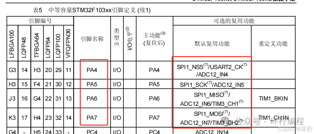
Wiring between STM32F103C8T6 and W25Q128:
| STM32 Pin | W25Q128 Pin | Function |
|---|---|---|
| PA5 | CLK | SPI Clock |
| PA6 | MISO | Master Input |
| PA7 | MOSI | Master Output |
| PA4 | CS | Chip Select Signal |
| 3.3V | VCC | Power Supply |
| GND | GND | Ground |
Note: The CS pin must be controlled by GPIO and cannot be fixed to low level
3. Code Implementation
3.1 SPI and GPIO Initialization
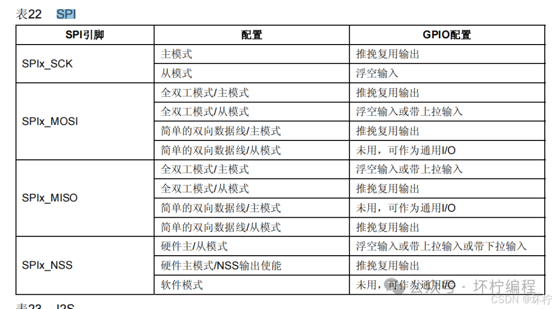
During initialization, we need to refer to the reference manual:Configure the GPIO ports according to the manual and actual situation
SPI_HandleTypeDef spi_handle = {0};
void w25q128_spi_init(void)
{
    spi_handle.Instance = SPI1;
    spi_handle.Init.Mode = SPI_MODE_MASTER;
    spi_handle.Init.Direction = SPI_DIRECTION_2LINES;
    spi_handle.Init.DataSize = SPI_DATASIZE_8BIT;
    spi_handle.Init.CLKPolarity = SPI_POLARITY_LOW;              /* CPOL = 0 */
    spi_handle.Init.CLKPhase = SPI_PHASE_1EDGE;                  /* CPHA = 0 */
    spi_handle.Init.NSS = SPI_NSS_SOFT;
    spi_handle.Init.BaudRatePrescaler = SPI_BAUDRATEPRESCALER_256;
    spi_handle.Init.FirstBit = SPI_FIRSTBIT_MSB;
    spi_handle.Init.TIMode = SPI_TIMODE_DISABLE;
    spi_handle.Init.CRCCalculation = SPI_CRCCALCULATION_DISABLE;
    spi_handle.Init.CRCPolynomial = 7;
    HAL_SPI_Init(&spi_handle);
}

void HAL_SPI_MspInit(SPI_HandleTypeDef *hspi)
{
    if(hspi->Instance == SPI1)
    {
        GPIO_InitTypeDef gpio_initstruct;
        // Enable clock
        __HAL_RCC_GPIOA_CLK_ENABLE();                           // Enable GPIOB clock
        __HAL_RCC_SPI1_CLK_ENABLE();

        // Call GPIO initialization function
        gpio_initstruct.Pin = GPIO_PIN_4;
        gpio_initstruct.Mode = GPIO_MODE_OUTPUT_PP;
        gpio_initstruct.Pull = GPIO_PULLUP;
        gpio_initstruct.Speed = GPIO_SPEED_FREQ_HIGH;
        HAL_GPIO_Init(GPIOA,&gpio_initstruct);

        gpio_initstruct.Pin = GPIO_PIN_5 | GPIO_PIN_7;
        gpio_initstruct.Mode = GPIO_MODE_AF_PP;
        HAL_GPIO_Init(GPIOA,&gpio_initstruct);

        gpio_initstruct.Pin = GPIO_PIN_6;
        gpio_initstruct.Mode = GPIO_MODE_INPUT;
        HAL_GPIO_Init(GPIOA,&gpio_initstruct);
    }
}
3.2 W25Q128 Driver Functions
w251128.c
// Swap a byte
uint8_t w25q128_spi_swap_byte(uint8_t data)
{
    uint8_t recv_data = 0;
    HAL_SPI_TransmitReceive(&spi_handle, &data, &recv_data, 1, 1000);
    return recv_data;
}

// Initialization:
void w25q128_init(void)
{
    w25q128_spi_init();
}

// Read ID value
uint16_t w25q128_read_id(void)
{
    uint16_t device_id = 0;
    W25Q128_CS(0);

    w25q128_spi_swap_byte(FLASH_ManufactDeviceID);
    w25q128_spi_swap_byte(0x00);
    w25q128_spi_swap_byte(0x00);
    w25q128_spi_swap_byte(0x00);
    device_id = w25q128_spi_swap_byte(FLASH_DummyByte) << 8;
    device_id |= w25q128_spi_swap_byte(FLASH_DummyByte);

    W25Q128_CS(1);
    return device_id;
}

// Write Enable
void w25q128_write_enable(void)
{
    W25Q128_CS(0);
    w25q128_spi_swap_byte(FLASH_WriteEnable);
    W25Q128_CS(1);
}

// Read Status Register 1
uint8_t w25q128_read_sr1(void)
{
    uint8_t recv_data = 0;

    W25Q128_CS(0);
    w25q128_spi_swap_byte(FLASH_ReadStatusReg1);
    recv_data = w25q128_spi_swap_byte(FLASH_DummyByte);
    W25Q128_CS(1);

    return recv_data;
}

// Wait for BUSY
void w25q128_wait_busy(void)
{
    while((w25q128_read_sr1() & 0x01) == 0x01);
}
// Send address
void w25q128_send_address(uint32_t address)
{
    w25q128_spi_swap_byte(address >> 16);
    w25q128_spi_swap_byte(address >> 8);
    w25q128_spi_swap_byte(address);
}
// Read data
void w25q128_read_data(uint32_t address, uint8_t* data, uint32_t size)
{
    uint32_t i = 0;
    W25Q128_CS(0);
    w25q128_spi_swap_byte(FLASH_ReadData);
    w25q128_send_address(address);

    for(i = 0; i < size; i++)
        data[i] = w25q128_spi_swap_byte(FLASH_DummyByte);
    W25Q128_CS(1);
}
// Page Write
void w25q128_write_page(uint32_t address, uint8_t* data, uint16_t size)
{
    uint16_t i = 0;
    w25q128_write_enable();

    W25Q128_CS(0);
    w25q128_spi_swap_byte(FLASH_PageProgram);
    w25q128_send_address(address);

    for(i = 0; i < size; i++)
        w25q128_spi_swap_byte(data[i]);

    W25Q128_CS(1);
    // Wait for idle
    w25q128_wait_busy();
}
// Erase
void w25q128_erase_sector(uint32_t address)
{
    // Write Enable
    w25q128_write_enable();
    // Wait for idle
    w25q128_wait_busy();
    // Pull CS low
    W25Q128_CS(0);
    // Send sector erase command
    w25q128_spi_swap_byte(FLASH_SectorErase);
    // Send address
    w25q128_send_address(address);
    // Pull CS high
    W25Q128_CS(1);
    // Wait for idle
    w25q128_wait_busy();
}
w25q128.h
#ifndef __W25Q128_H__
#define __W25Q128_H__

#include "sys.h"

#define W25Q128_CS(x)   do{ x ? \
                                HAL_GPIO_WritePin(GPIOA, GPIO_PIN_4, GPIO_PIN_SET): \
                                HAL_GPIO_WritePin(GPIOA, GPIO_PIN_4, GPIO_PIN_RESET); \
                        }while(0)

/* Command Table */
#define FLASH_ManufactDeviceID                  0x90
#define FLASH_WriteEnable                       0x06
#define FLASH_ReadStatusReg1                    0x05
#define FLASH_ReadData                          0x03
#define FLASH_PageProgram                       0x02
#define FLASH_SectorErase                       0x20
#define FLASH_DummyByte                         0xFF

void w25q128_init(void);
uint16_t w25q128_read_id(void);
void w25q128_read_data(uint32_t address, uint8_t* data, uint32_t size);
void w25q128_write_page(uint32_t address, uint8_t* data, uint16_t size);
void w25q128_erase_sector(uint32_t address);

#endif
3.3 Usage Example
#include "sys.h"
#include "delay.h"
#include "led.h"
#include "uart1.h"
#include "w25q128.h"

uint8_t data_write[4] = {0xAA, 0xBB, 0xCC, 0xDD};
uint8_t data_read[4] = {0};
int main(void)
{
    HAL_Init();                         /* Initialize HAL library */
    stm32_clock_init(RCC_PLL_MUL9);     /* Set clock to 72MHz */
    led_init();                         /* Initialize LED */
    uart1_init(115200);
    w25q128_init();
    printf("hello world!\r\n");

    uint16_t device_id = w25q128_read_id();
    printf("device id: %X\r\n", device_id);

//    w25q128_erase_sector(0x000000);
//    w25q128_write_page(0x000000, data_write, 4);
    w25q128_read_data(0x000000, data_read, 4);

    printf("data read: %X, %X, %X, %X\r\n", data_read[0], data_read[1], data_read[2], data_read[3]);
    while(1)
    {

    }
}
4. Precautions
- Erase operation is mandatory: The Flash must be erased in the corresponding area before writing
- Page boundary limitation: Single write cannot cross pages (each page is 256 bytes)
- Clock configuration: Ensure the SPI clock does not exceed chip specifications (initially use a lower frequency)
- Status detection: Check the BUSY bit after important operations
- Power stability: Maintain a stable 3.3V during Flash operations
5. Common Issue Troubleshooting
- Unable to read ID: Check SPI mode (CPOL=0/CPHA=0), confirm CS signal timing
- Write failure: Ensure the write enable command has been executed, check power voltage
- Data error: Pay attention to address alignment, eliminate SPI clock interference
Complete project code can be obtained from Gitee: https://gitee.com/bad-lemon/mcu-development-record.git
Implementation Effect: The above code can achieve read and write operations for W25Q128, with a measured write speed of up to 600KB/s and a read speed of 1.2MB/s (SPI clock 18MHz). This solution is suitable for IoT devices, data acquisition systems, and other scenarios requiring large-capacity non-volatile storage.