Table of Contents
-
Standard Version and Q1 Version
-
Schematic Diagram
-
Physical Diagram
-
Test Wiring
-
Default Power-On Test
-
STM32CubeMX Configuration
-
Adaptation of SLLC469 Driver Library
-
SPI Read ID Test
-
Steps to Send and Receive CAN Messages
-
MCAN and MRAM Configuration
-
CAN Send Test
-
CAN Receive Test
-
VCCOUT Direct 5V Test
-
Open Circuit, Short Circuit, and Busoff Test
-
Program Link
-
Discussion Group
Standard Version and Q1 Version
TCAN4550 is a CANFD controller with an integrated CANFD transceiver. There are standard and Q1 versions compliant with AEC-Q100, summarized as follows:
Standard Version:
- TCAN4550
- CANFD data rate 5Mbps (8Mbps)
- Bus fault protection voltage ±42V
- Supply voltage (VSUP) 6V–24V
- Operating temperature from -40°C to 125°C
- PIN3, GPO1, supports output only
Q1 Version:
- TCAN4550-Q1
- CANFD data rate 8Mbps
- Bus fault protection voltage ±58V
- Supply voltage (VSUP) 5.5V–30V
- AEC-Q100 temperature grade 1, -40°C to 125°C, TA
- PIN3, GPIO1, can be configured as input/output via SPI
Other common features:
- PIN16, VCCOUT, provides 5V with a current of 70mA
- SPI clock rate up to 18Mbps
This article tests the Q1 version, with the chip marking <span>TCAN 4550Q1</span> and model TCAN4550RGYRQ1, as shown in the figure below:
Schematic Diagram
Physical Diagram
Introduction as follows:
- On the left is a 2.54-2x5P IDC connector (horn connector), which can also plug in Dupont wires
- On the right is a 3.5mm-4P terminal
- VSUP external power supply 5.5~30V
- Marked with TCAN4550RGYRQ1, external 40MHz passive crystal oscillator
- Three indicator lights indicate VIO, VCCOUT, and VSUP
- Onboard 120Ω termination resistor
Test Wiring
In case of uncertainty, using the STM32G431CBT6 as the test board, the pin connection is as follows:
- PA4, SPI1_nCS
- PA5, SPI1_SCK
- PA6, SPI1_MISO
- PA7, SPI1_MOSI
- PC4, TCAN_RST (high level reset)
- PB0, TCAN_nINT (falling edge interrupt, EXTI0)
Additionally, VIO (connected to 3.3V) and GND are used, totaling 8 pins on the left side of the TCAN4550 board.
On the right, VSUP and GND connect to the power supply (5.5V~30V), CANH and CANL connect to the device or CANFD analyzer.
Default Power-On Test
If the MCU is not connected, or if the MCU is not powered, only supplying power to the board’s VSUP:
- It can be observed that the VSUP and VCCOUT indicator lights are on
- The measured voltage of VCCOUT is 5V
- If VSUP drops to 5.4V or below, VCCOUT goes out, and the board cannot function properly
- After 4 minutes, the VCCOUT indicator light automatically goes out, and the board enters Sleep mode
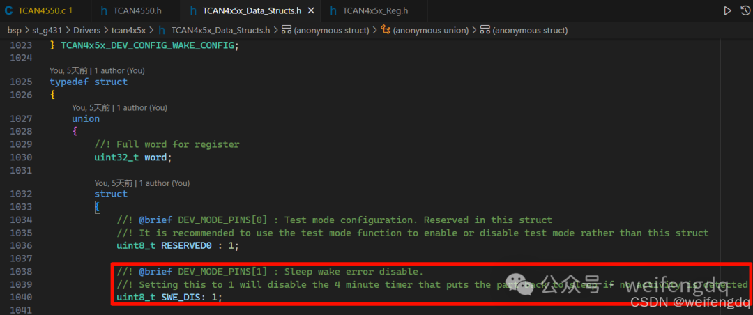
The last point is also mentioned in the manual and should be noted:
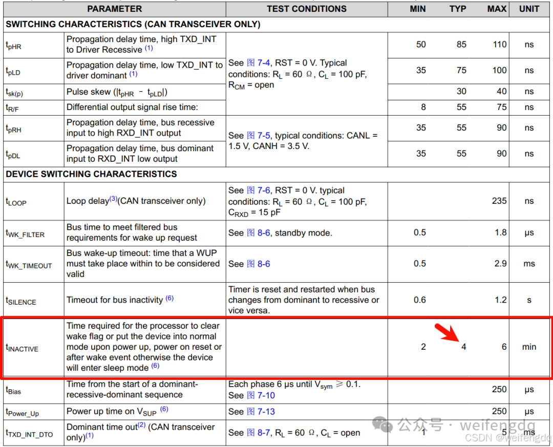
After power-on reset, it first enters Standby Mode, and after 4 minutes of inactivity, it enters Sleep Mode, where VCCOUT no longer outputs 5V, and SPI can no longer function unless CAN or the WAKE pin wakes it up:
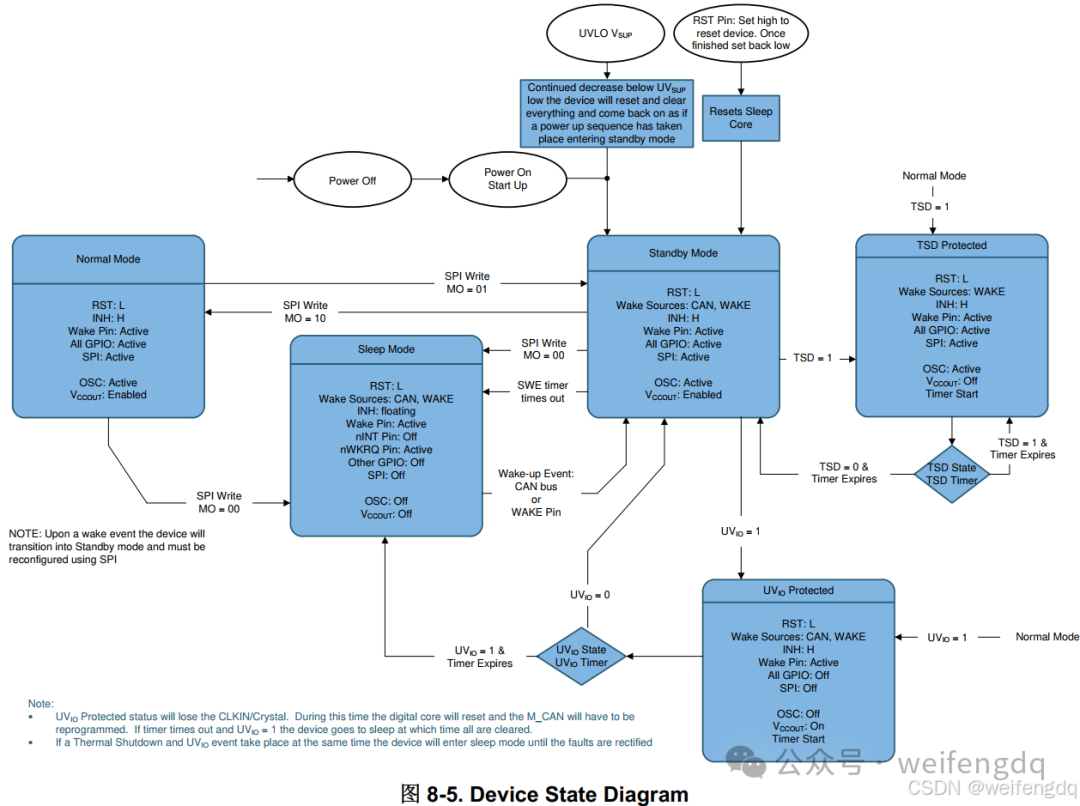
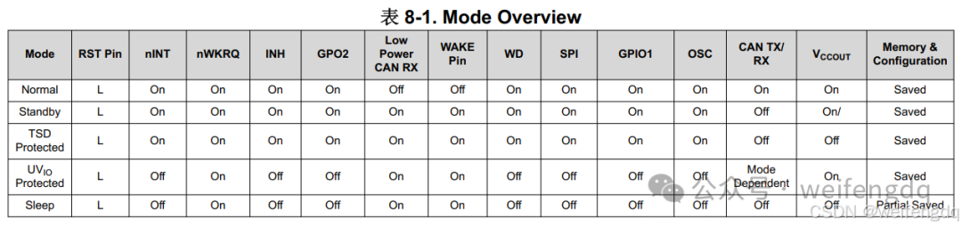
Performance of various pins in different modes:
For simplicity in testing, the SWE_DIS bit of register 0x0800 can be turned off
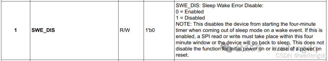
The driver library also has this explanation
Example usage:
TCAN4x5x_DEV_CONFIG devCfg;
TCAN4x5x_Device_ReadConfig(&devCfg);
devCfg.SWE_DIS = 1;
if (!TCAN4x5x_Device_Configure(&devCfg)) {
  printf("Failed to configure device\n");
}
Later, the watchdog is also turned off for testing convenience.
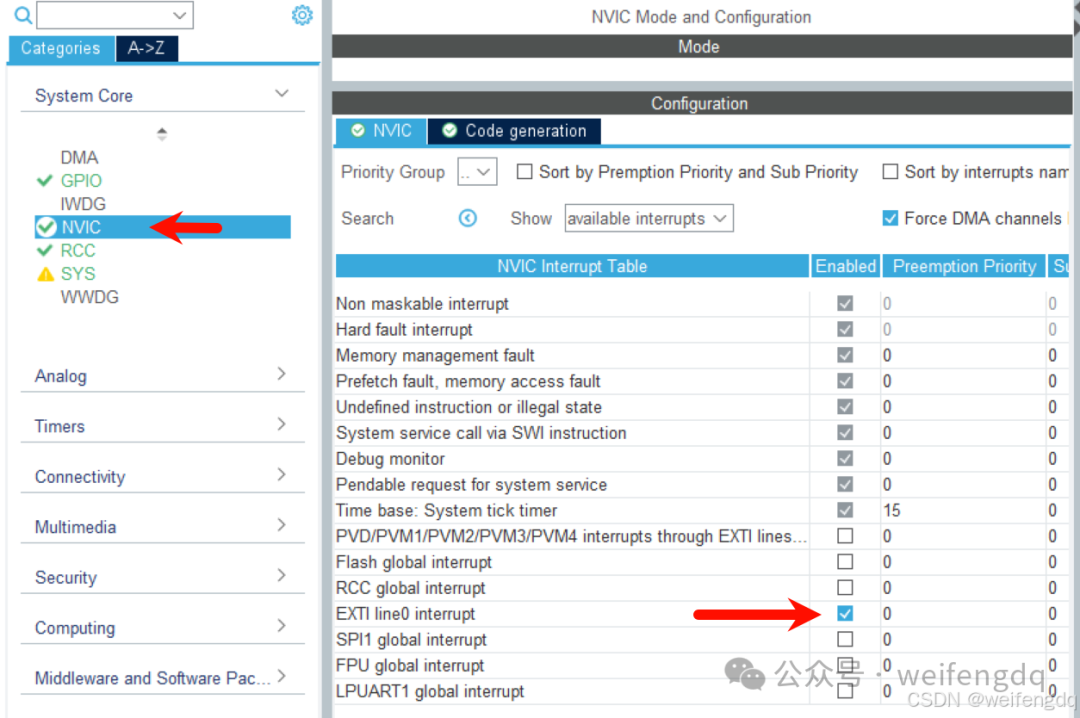
STM32CubeMX Configuration
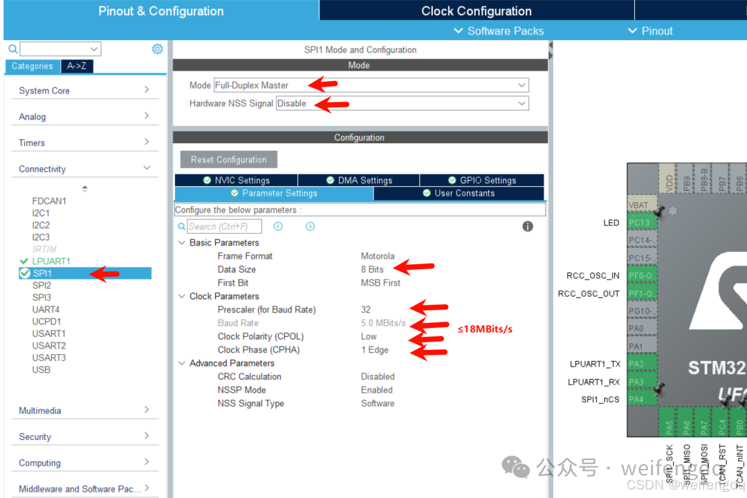
SPI mode 0, full duplex, software chip select, data 8 bits, not exceeding 18Mbits/s, here is a 160MHz system clock, after 32 division it is 5Mbits/s, it is recommended to use above 10Mbits/s to prevent packet loss under high load.
Chip select is high level by default
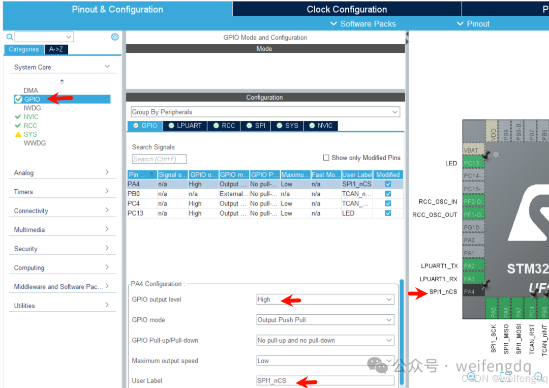
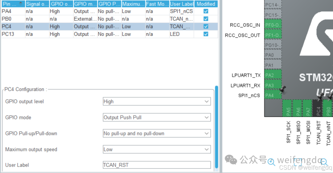
Reset is high level by default (reset)
Falling edge interrupt (the board has a 10K pull-up resistor)
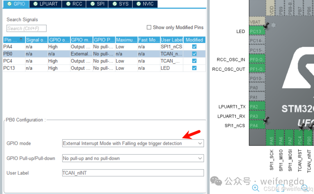
Enable EXTI0 interrupt
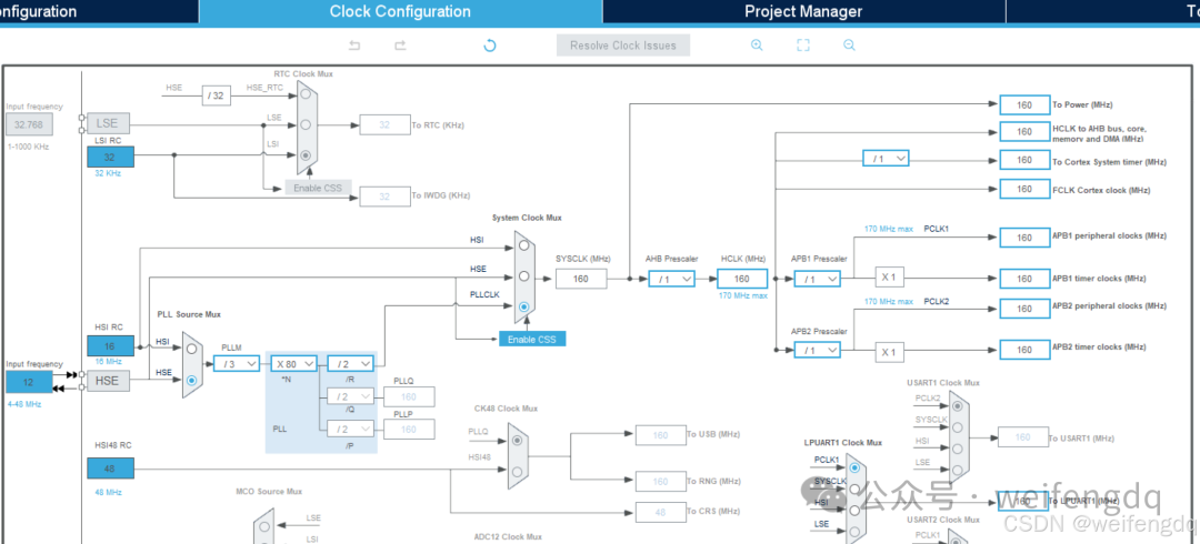
External clock 12M passive crystal oscillator, system clock 160MHz
Other LED, UART, Debug, project generation omitted.
Adaptation of SLLC469 Driver Library
SLLC469 driver or library | Texas Instruments TI.com.cn, the examples inside are for MSP430, mainly to adapt the 8 functions of TCAN4x5x_SPI for STM32:
void AHB_WRITE_32(uint16_t address, uint32_t data);
void AHB_WRITE_BURST_START(uint16_t address, uint8_t words);
void AHB_WRITE_BURST_WRITE(uint32_t data);
void AHB_WRITE_BURST_END(void);

uint32_t AHB_READ_32(uint16_t address);
void AHB_READ_BURST_START(uint16_t address, uint8_t words);
uint32_t AHB_READ_BURST_READ(void);
void AHB_READ_BURST_END(void);
Taking <span>AHB_WRITE_32</span> and <span>AHB_READ_BURST_*</span> as examples, replace the original with ST’s chip select and SPI send/receive functions:
void AHB_WRITE_32(uint16_t address, uint32_t data) {
uint8_t buffer[8];
  buffer[0] = AHB_WRITE_OPCODE;  // 0x61
  buffer[1] = (address >> 8) & 0xFF;
  buffer[2] = address & 0xFF;
  buffer[3] = 0x01;
  buffer[4] = (data >> 24) & 0xFF;
  buffer[5] = (data >> 16) & 0xFF;
  buffer[6] = (data >> 8) & 0xFF;
  buffer[7] = data & 0xFF;
  HAL_GPIO_WritePin(SPI1_nCS_GPIO_Port, SPI1_nCS_Pin, GPIO_PIN_RESET);
  HAL_StatusTypeDef status = HAL_SPI_Transmit(&hspi1, buffer, 8, 1000);
  HAL_GPIO_WritePin(SPI1_nCS_GPIO_Port, SPI1_nCS_Pin, GPIO_PIN_SET);
if (status != HAL_OK) {
    print("AHB_WRITE_32 Error: %d\n", (int)status);
  }
}

void AHB_READ_BURST_START(uint16_t address, uint8_t words) {
uint8_t tx_buf[4] = {0};
  tx_buf[0] = AHB_READ_OPCODE;
  tx_buf[1] = (address >> 8) & 0xFF;
  tx_buf[2] = address & 0xFF;
  tx_buf[3] = words;
  HAL_GPIO_WritePin(SPI1_nCS_GPIO_Port, SPI1_nCS_Pin, GPIO_PIN_RESET);
  HAL_StatusTypeDef status = HAL_SPI_Transmit(&hspi1, tx_buf, 4, 1000);
if (status != HAL_OK) {
    print("AHB_READ_BURST_START Error: %d\n", (int)status);
  }
}

uint32_t AHB_READ_BURST_READ(void) {
uint32_t ret;
uint8_t rx_buf[4] = {0};
  HAL_StatusTypeDef status = HAL_SPI_Receive(&hspi1, rx_buf, 4, 1000);
if (status != HAL_OK) {
    print("AHB_READ_BURST_READ Error: %d\n", (int)status);
  }
  ret = ((uint32_t)rx_buf[0] << 24) | ((uint32_t)rx_buf[1] << 16) |
               ((uint32_t)rx_buf[2] << 8) | rx_buf[3];
return ret;
}

void AHB_READ_BURST_END(void) {
  HAL_GPIO_WritePin(SPI1_nCS_GPIO_Port, SPI1_nCS_Pin, GPIO_PIN_SET);
}
SPI Read ID Test
Generally, the ID register is used to test whether the SPI communication configuration is normal:
The SPI read composition is the host sending a four-byte read opcode (0x41) + 16-bit address + the length of the word to read (bits/32)
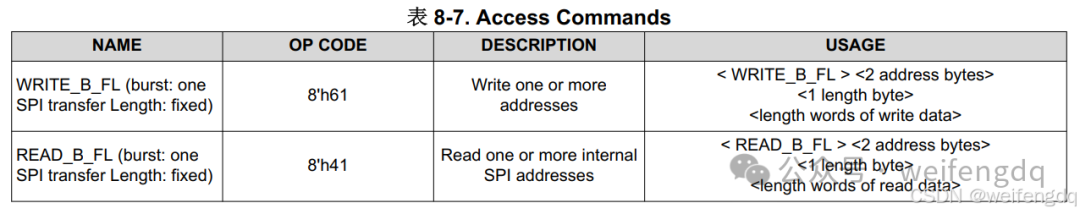
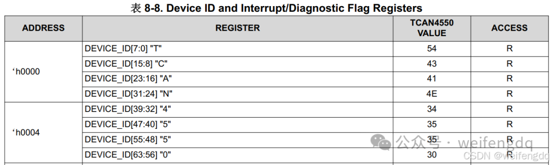
Taking registers 0 and 4 as examples, read out TCAN4550, below is the waveform captured by the logic analyzer:
Here, each time a register (32bit) is read, it can also be <span>41 00 00 02</span> to read two registers at once
Steps to Send and Receive CAN Messages
To use TCAN4550-Q1 to transmit messages, the following operations must be completed:
- Ensure that TCAN4550-Q1 is in standby mode (register 0x0800[7:6]=0’b01). This forces M_CAN into INIT mode.
- Set the M_CAN CCR register to allow configuration. If not set, set the CCE and INIT bits. Note: In standby mode, the CSR bit reads back as 1, but the user must write 0 to this bit when performing a read-modify-write; otherwise, CAN communication will fail.
- If CANFD and Bit Rate Switching (BRS) support is needed, it must be globally enabled during configuration via the FDF and BRS bits in the CCR register. For more information on this register, refer to the device datasheet.
- Any required device functions, such as watchdog timers, should be configured.
- CAN timing information must be set.
- Any data can be used to configure and initialize the MRAM section.
- Put the TCAN4550-Q1 device into “normal” mode (register 0x0800[7:6]=0’b10) to enable the transceiver and allow the CAN core to transmit.
- After completing these steps, the microcontroller will be able to transmit messages by writing to the TX buffer and then requesting to send the message by writing to the TXBAR register.
MCAN and MRAM Configuration
TCAN4550 register allocation:
- Register 16’h0000 through 16’h000C are Device ID and SPI Registers
- Register 16’h0800 through 16’h083C are device configuration registers and Interrupt Flags
- Register 16’h1000 through 16’h10FC are for M_CAN
- Register 16’h8000 through 16’h87FF is for MRAM.
Similar to STM32H7 or TC397, TCAN4550 is also MCAN, with 2KB of Message RAM, and the configuration is quite similar:
- Taking the longest 64-byte CANFD frame as an example, along with ID flags, it requires 72 bytes of MRAM. The maximum 2KB can support
<span>2048/72 =28.44</span>transceivers, but at least one standard frame and one extended frame filter (mask method to receive all) space must be reserved, allowing for 27 transceivers. - If receiving is placed in a while loop, then more RX FIFO is needed. For example, if the while loop can guarantee a 1ms cycle, all are 64-byte CANFD frames, at 5Mbit/s, a maximum of 8 frames can be processed in 1ms, so here 11 RX FIFO depth is given. If the frames are shorter, the number of messages is more, and processing in 1ms may require deeper FIFO, or reduce the longest 64 to allow more RX, or directly read the data in the nINT interrupt and throw it into its own software FIFO to avoid loss.
- Sending is similar; MCAN generally has a maximum of 32 Buffers or FIFOs, here 17 are given, meaning that the MCU (160MHz fill speed is fast, but CAN’s 5Mbit/s sending speed is slow) should not send more than 17 frames at once. It can send an interrupt to fill the next frame, or to be more convenient, fill no more than 4 frames in 1ms.
- FIFO and Buffer are of course best to have more; if it is known that all data lengths do not exceed 8 bytes, 2KB can be divided into up to
<span>2048/16=128</span>, filling the TX with 32, and the rest for RX, or TX data 8 bytes, RX data 64 bytes, all are possible, as long as there is no overlap or out of bounds. If insufficient, directly take it in the receive interrupt to its own software FIFO or take data from its own send FIFO in the send interrupt, which is equivalent to managing flow control by oneself. - With a 40MHz clock, generally the arbitration segment is not divided or divided by 4 to 10MHz, the data segment is not divided, and the sample point is conveniently calculated as 80%. There will not be major issues interfacing with others at 75% or 87.5%. The main concern is when exceeding 2Mbit/s, adjust the transceiver parameters to tune TDC, which may not need adjustment (automatically calculated based on parameters like Tseg).
Configuration code example is as follows:
- Enabled low voltage, short circuit, open circuit, and Busoff interrupts
- Enabled FDF and BRS for CANFD support (does not affect sending ordinary CAN messages, like a person having the ability to run but not affecting walking)
- Automatically calculated Tq parameters based on baud rate and sample point (only tested [email protected], [email protected])
- A standard frame filter (each occupying 4 bytes of MRAM, register address 0x8000), mask method, receives all into RXFIFO0
- An extended frame filter (each occupying 8 bytes of MRAM, register address 0x8004), mask method, receives all into RXFIFO0
- 11 RX FIFO0 capable of receiving 64-byte CANFD data (each occupying 72 bytes of MRAM, register addresses 0x800C, 0x800C, 0x809C, …, 0x82DC), can also receive frames of length
<span>[0, 1, 2, 3, 4, 5, 6, 7, 8, 12, 16, 20, 24, 32, 48, 64]</span>. - 16 TX Buffers capable of sending 64-byte CANFD data (each occupying 72 bytes of MRAM, register addresses 0x8324, 0x836C, …, 0x875C), can also send frames of length
<span>[0, 1, 2, 3, 4, 5, 6, 7, 8, 12, 16, 20, 24, 32, 48, 64]</span>for ordinary CAN, CANFD, CANFD with BRS - Remaining 0x800 – 0x7A4 = 0x5C = 92 bytes of RAM unused
void tcan4x5x_mcan_config(uint32_t baud, float sample_point,
                                 uint32_t data_baud, float data_sample_point) {
// Disable all non-MCAN related interrupts for simplicity
  TCAN4x5x_Device_Interrupt_Enable ie = {0};
  ie.UVIOEN = 1;           // UVIO, Undervoltage on VIO
  ie.UVSUPEN = 1;          // UVSUP, Undervoltage on VSUP and VCCOUT
  ie.CANBUSBATEN = 1;      // CANBUSBAT, CAN Shorted to VBAT
  ie.CANBUSGNDEN = 1;      // CANBUSGND, CAN Shorted to GND
  ie.CANBUSOPENEN = 1;     // CANBUSOPEN, CAN Open fault
  ie.CANLGNDEN = 1;        // CANLGND, CANL GND
  ie.CANHBATEN = 1;        // CANHBAT, CANH to VBAT
  ie.CANHCANLEN = 1;       // CANHCANL, CANH and CANL shorted
  ie.CANBUSTERMOPENEN = 1; // CANBUSTERMOPEN, CAN Bus has termination point open
  ie.CANBUSNORMEN = 1;     // CANBUSNOM, CAN Bus is normal flag
  TCAN4x5x_Device_ConfigureInterruptEnable(&ie);
// Clear PWRON because if it's not cleared within ~4 minutes, it goes to sleep
  TCAN4x5x_Device_Interrupts ir = {0};
  TCAN4x5x_Device_ReadInterrupts(&ir);
if (ir.PWRON) {
    TCAN4x5x_Device_ClearInterrupts(&ir);
    TCAN4x5x_Debug("Cleared PWRON interrupt\n");
  }

// 40MHz Clock
  TCAN4x5x_MCAN_CCCR_Config cccr_config = {0};
  cccr_config.FDOE = 1;  // FDF
  cccr_config.BRSE = 1;  // BRS
  TCAN4x5x_MCAN_Nominal_Timing_Simple timing = {
      .NominalBitRatePrescaler = 4,
      .NominalTqBeforeSamplePoint =
          (int)roundf((10000000.0f / baud) * sample_point),  // <math.h>
      .NominalTqAfterSamplePoint =
          (int)roundf((10000000.0f / baud) * (1 - sample_point));
  };
  TCAN4x5x_Debug("NominalTqBeforeSamplePoint: %d\n",
                 timing.NominalTqBeforeSamplePoint);
  TCAN4x5x_Debug("NominalTqAfterSamplePoint: %d\n",
                 timing.NominalTqAfterSamplePoint);
  TCAN4x5x_MCAN_Data_Timing_Simple data_timing = {
      .DataBitRatePrescaler = 1,
      .DataTqBeforeSamplePoint =
          (int)roundf((40000000 / data_baud) * data_sample_point),
      .DataTqAfterSamplePoint =
          (int)roundf((40000000 / data_baud) * (1 - data_sample_point));
  };
  TCAN4x5x_Debug("DataTqBeforeSamplePoint: %d\n",
                 data_timing.DataTqBeforeSamplePoint);
  TCAN4x5x_Debug("DataTqAfterSamplePoint: %d\n",
                 data_timing.DataTqAfterSamplePoint);
  TCAN4x5x_MCAN_Global_Filter_Configuration global_filter = {0};
  global_filter.RRFE = 1;
  global_filter.RRFS = 1;
  global_filter.ANFE = TCAN4x5x_GFC_ACCEPT_INTO_RXFIFO0;
  global_filter.ANFS = TCAN4x5x_GFC_ACCEPT_INTO_RXFIFO0;
// 2KB MRAM, 2048 / 72 = 28.44
  TCAN4x5x_MRAM_Config mram_config = {
      .SIDNumElements = 1,
      .XIDNumElements = 1,
      .Rx0NumElements = 11,
      .Rx0ElementSize = MRAM_64_Byte_Data,
      .Rx1NumElements = 0,
      .Rx1ElementSize = MRAM_64_Byte_Data,
      .RxBufNumElements = 0,
      .RxBufElementSize = MRAM_64_Byte_Data,
      .TxEventFIFONumElements = 0,
      .TxBufferNumElements = 16,
      .TxBufferElementSize = MRAM_64_Byte_Data,
  };

  TCAN4x5x_MCAN_EnableProtectedRegisters();
  TCAN4x5x_MCAN_ConfigureCCCRRegister(&cccr_config);
  TCAN4x5x_MCAN_ConfigureGlobalFilter(&global_filter);
  TCAN4x5x_MCAN_ConfigureNominalTiming_Simple(&timing);
  TCAN4x5x_MCAN_ConfigureDataTiming_Simple(&data_timing);
  TCAN4x5x_MRAM_Clear();
  TCAN4x5x_MRAM_Configure(&mram_config);
  TCAN4x5x_MCAN_DisableProtectedRegisters();

// interrupt
  TCAN4x5x_MCAN_Interrupt_Enable mcan_ie = {0};
  mcan_ie.RF0NE = 1; // Enable RX FIFO 0 New Message interrupt
  mcan_ie.EPE = 1;   // Enable Error Passive interrupt
  mcan_ie.EWE = 1;   // Enable Warning Status interrupt
  mcan_ie.BOE = 1;   // Enable Bus Off interrupt
  TCAN4x5x_MCAN_ConfigureInterruptEnable(&mcan_ie);

// filter
  TCAN4x5x_MCAN_SID_Filter std_filter = {0};
  std_filter.SFT = TCAN4x5x_SID_SFT_CLASSIC;
  std_filter.SFEC = TCAN4x5x_SID_SFEC_PRIORITYSTORERX0;
  std_filter.SFID1 = 0;
  std_filter.SFID2 = 0;
  TCAN4x5x_MCAN_WriteSIDFilter(0, &std_filter);
  TCAN4x5x_MCAN_XID_Filter ext_filter = {0};
  ext_filter.EFT = TCAN4x5x_XID_EFT_CLASSIC;
  ext_filter.EFEC = TCAN4x5x_XID_EFEC_PRIORITYSTORERX0;
  ext_filter.EFID1 = 0;
  ext_filter.EFID2 = 0;
  TCAN4x5x_MCAN_WriteXIDFilter(0, &ext_filter);

/* Configure the TCAN4550 Non-CAN-related functions */
  TCAN4x5x_DEV_CONFIG devConfig = {0};
  devConfig.SWE_DIS =
      0; // Keep Sleep Wake Error Enabled (it's a disable bit, not an enable)
  devConfig.DEVICE_RESET = 0; // Not requesting a software reset
  devConfig.WD_EN = 0;        // Watchdog disabled
  devConfig.nWKRQ_CONFIG = 0; // Mirror INH function (default)
  devConfig.INH_DIS = 0;      // INH enabled (default)
  devConfig.GPIO1_GPO_CONFIG =
      TCAN4x5x_DEV_CONFIG_GPO1_MCAN_INT1; // MCAN nINT 1 (default)
  devConfig.FAIL_SAFE_EN = 0;             // Failsafe disabled (default)
  devConfig.GPIO1_CONFIG =
      TCAN4x5x_DEV_CONFIG_GPIO1_CONFIG_GPO; // GPIO set as GPO (Default)
  devConfig.WD_ACTION =
      TCAN4x5x_DEV_CONFIG_WDT_ACTION_nINT; // Watchdog set an interrupt
                                           // (default)
  devConfig.WD_BIT_RESET = 0;              // Don't reset the watchdog
  devConfig.nWKRQ_VOLTAGE = 0; // Set nWKRQ to internal voltage rail (default)
  devConfig.GPO2_CONFIG =
      TCAN4x5x_DEV_CONFIG_GPO2_NO_ACTION; // GPO2 has no behavior (default)
  devConfig.CLK_REF = 1; // Input crystal is a 40 MHz crystal (default)
  devConfig.WAKE_CONFIG =
      TCAN4x5x_DEV_CONFIG_WAKE_BOTH_EDGES; // Wake pin can be triggered by
                                           // either edge (default)
  TCAN4x5x_Device_Configure(&devConfig);

  TCAN4x5x_Device_SetMode(TCAN4x5x_DEVICE_MODE_NORMAL);
  TCAN4x5x_MCAN_ClearInterruptsAll();
}
As an example of the configuration commonly used in robot motor control of [email protected], [email protected], the automatically calculated results are:
# tcan4x5x_mcan_config(1000000, 0.8f, 5000000, 0.75f);
NominalTqBeforeSamplePoint: 8
NominalTqAfterSamplePoint: 2
DataTqBeforeSamplePoint: 6
DataTqAfterSamplePoint: 2
CAN Send Test
Send in the form of the above configuration Buffer, here sending every 10ms, can be encapsulated into a structure similar to SocketCAN, as follows:
void tcan4x5x_mcan_write_test_2(void) {
static uint32_t last_send_time = 0;
static uint64_t counter = 0;
uint32_t current_time = HAL_GetTick();

if (is_busoff_or_error) {
    return;
  }

// Send message every 1ms
if (current_time - last_send_time >= 1) {
    // Prepare TX header with ID 0x456
    TCAN4x5x_MCAN_TX_Header tx_header = {
        .ID = 0x456,
        .RTR = 0,
        .XTD = 0,
        .ESI = 0,
        .DLC = 8, // 8 bytes for uint64_t
        .BRS = 0,
        .FDF = 0,
        .reserved = 0,
        .EFC = 0,
        .MM = 0,
    };

    // Convert uint64_t counter to byte array (little-endian)
    uint8_t data[8];
    data[0] = (uint8_t)(counter);
    data[1] = (uint8_t)(counter >> 8);
    data[2] = (uint8_t)(counter >> 16);
    data[3] = (uint8_t)(counter >> 24);
    data[4] = (uint8_t)(counter >> 32);
    data[5] = (uint8_t)(counter >> 40);
    data[6] = (uint8_t)(counter >> 48);
    data[7] = (uint8_t)(counter >> 56);

    // Get next buffer index
    static uint8_t buffer_index = 0;
    buffer_index = (buffer_index + 1) % 16;

    // Write to TX buffer and transmit
    if (TCAN4x5x_MCAN_WriteTXBuffer(buffer_index, &tx_header, data)) {
      if (TCAN4x5x_MCAN_TransmitBufferContents(buffer_index)) {
        // TCAN4x5x_Debug("Sent ID 0x456, counter: %llu\n", counter);
        counter++;
        last_send_time = current_time;
      } else {
        TCAN4x5x_Debug("Failed to transmit buffer\n");
      }
    }
  }
}
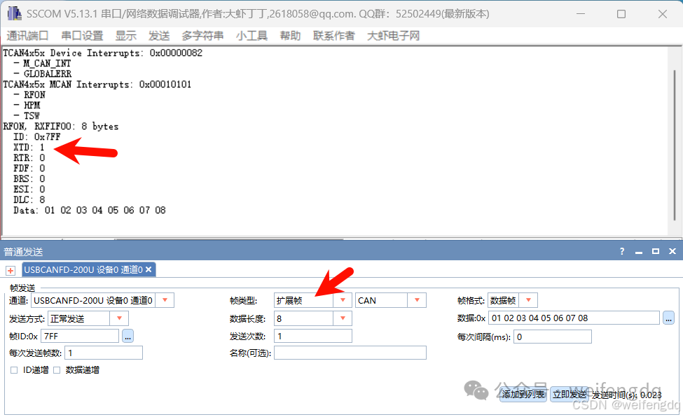
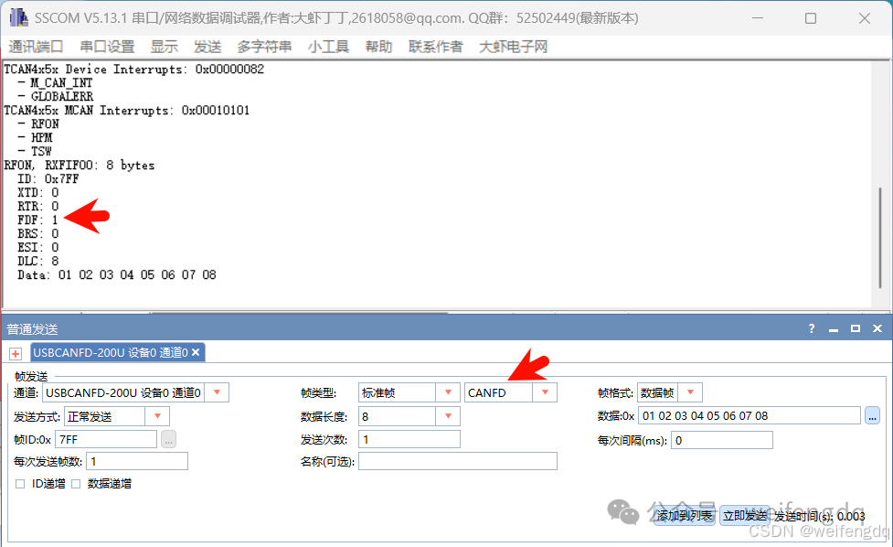
Note:
- Set extended frame XTD to 1
- To send CANFD frames, set FDF and BRS to 1
- DLC corresponds to lengths [0,15] for [0, 1, 2, 3, 4, 5, 6, 7, 8, 12, 16, 20, 24, 32, 48, 64].
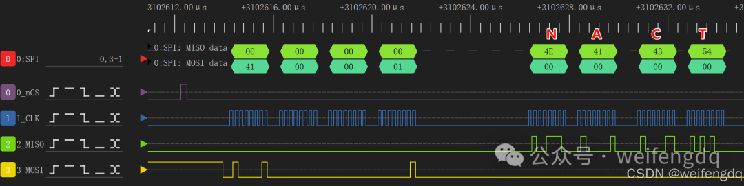
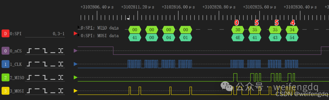
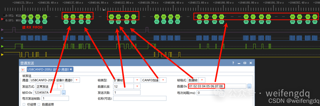
Thus, messages can be received at a 1ms cycle as follows:
Waveform captured by the logic analyzer:
-
The first write corresponds to
<span>TCAN4x5x_MCAN_WriteTXBuffer(buffer_index, &tx_header, data)</span> -
61, write opcode
-
8324, reference above MRAM, is the address of the configured TX Buffer0
-
04, length of 4 words
-
0x11580000, calculation method reference
-
SPIData = 0; SPIData |= ((uint32_t)header->ESI & 0x01) << 31; SPIData |= ((uint32_t)header->XTD & 0x01) << 30; SPIData |= ((uint32_t)header->RTR & 0x01) << 29; if (header->XTD) SPIData |= ((uint32_t)header->ID & 0x1FFFFFFF); else SPIData |= ((uint32_t)header->ID & 0x07FF) << 18; // 0x456 << 18 = 0x11580000 -
Flag 0x00080000, reference
-
SPIData = 0; SPIData |= ((uint32_t)header->DLC & 0x0F) << 16; SPIData |= ((uint32_t)header->BRS & 0x01) << 20; SPIData |= ((uint32_t)header->FDF & 0x01) << 21; SPIData |= ((uint32_t)header->EFC & 0x01) << 23; SPIData |= ((uint32_t)header->MM & 0xFF) << 24; // DLC = 8, check table [0, 1, 2, 3, 4, 5, 6, 7, 8, 12, 16, 20, 24, 32, 48, 64], data length 8 bytes -
Data
<span>0F 00 00 00 00 00 00 00</span> -
The next write corresponds to
<span>TCAN4x5x_MCAN_TransmitBufferContents(0)</span>, 10D0 is<span>REG_MCAN_TXBAR</span>register, 32bit corresponds to a maximum of 32 buffers, here it sends out the contents of TX Buffer0, just 1 << 0
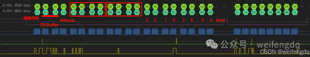
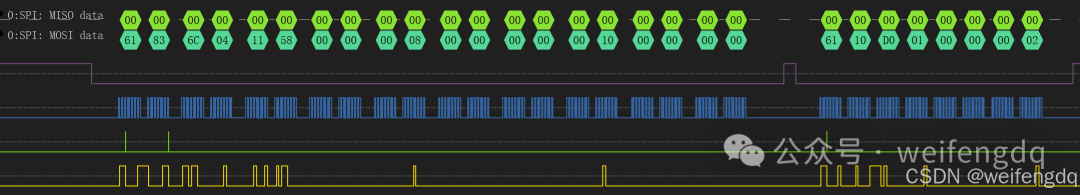
The waveform of the next frame, TX Buffer1, data <span>10 00 00 00 00 00 00 00</span>, sends out the contents of TX Buffer1 1 << 1
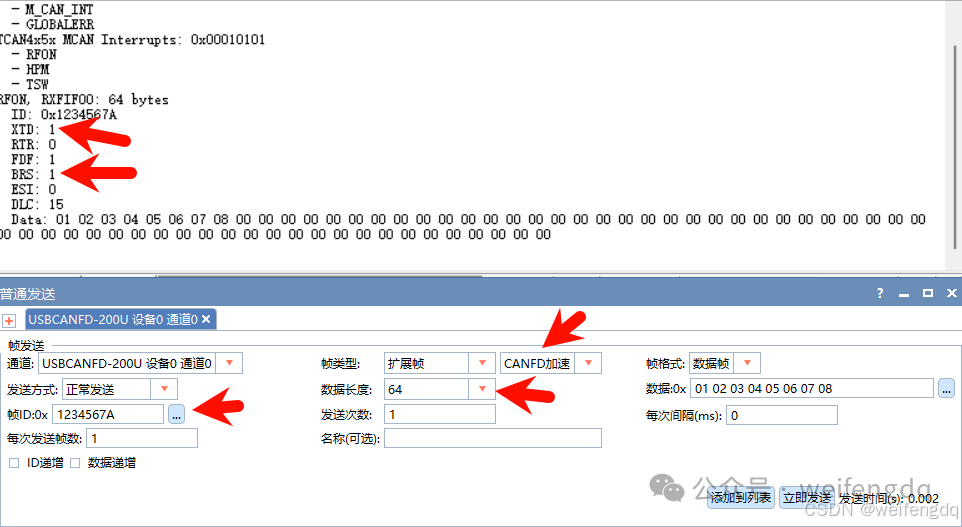
Make a slight modification
    TCAN4x5x_MCAN_TX_Header tx_header = {
        .ID = 0x12345678,
        .RTR = 0,
        .XTD = 1,
        .ESI = 0,
        .DLC = 15, // 64 bytes
        .BRS = 1,
        .FDF = 1,
        .reserved = 0,
        .EFC = 0,
        .MM = 0,
    };
    uint8_t data[64] = {0};
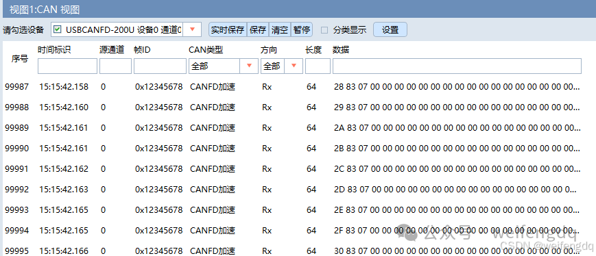
Received
CAN Receive Test
nINT has enabled the new message interrupt, and the main loop processes the interrupt and prints:
static int interrupt_count = 0;
void HAL_GPIO_EXTI_Callback(uint16_t GPIO_Pin) {
if (GPIO_Pin == GPIO_PIN_0) {
    interrupt_count++;
    HAL_GPIO_TogglePin(LED_GPIO_Port, LED_Pin);
  }
}

void bsp_tcan4x5x_process(void) {
// if busoff or error, wait 100ms and reinit
if (busoff_or_error_count && HAL_GetTick() - busoff_or_error_count > 100) {
    TCAN4x5x_Debug("busoff_or_error_count: %d\n", busoff_or_error_count);
    busoff_or_error_count = 0;
    bsp_tcan4x5x_init();
  }
if (interrupt_count) {
    TCAN4x5x_Debug("interrupt_count: %d\n", interrupt_count);
    interrupt_count--;
    TCAN4x5x_Device_Interrupts dev_ir = {0};
    TCAN4x5x_Device_ReadInterrupts(&dev_ir);
    TCAN4x5x_Debug("TCAN4x5x Device Interrupts: 0x%08X\n", dev_ir.word);
    int dev_interrupts_counter = 0;
    for (int i = 0; i < sizeof(dev_interrupts) / sizeof(dev_interrupts[0]);
         i++) {
      if (dev_ir.word & (1 << i)) {
        TCAN4x5x_Debug("  - %s\n", dev_interrupts[i]);
        dev_interrupts_counter++;
      }
    }
    if (dev_ir.UVSUP) {
      is_busoff_or_error = true;
      TCAN4x5x_Debug("UVSUP, is_busoff_or_error: %d\n", is_busoff_or_error);
      busoff_or_error_count = HAL_GetTick();
      return;
    }
    if (dev_ir.SPIERR) {
      TCAN4x5x_Debug("SPIERR\n");
      TCAN4x5x_Device_ClearSPIERR();
    }

    TCAN4x5x_MCAN_Interrupts mcan_ir = {0};
    TCAN4x5x_MCAN_ReadInterrupts(&mcan_ir);
    TCAN4x5x_Debug("TCAN4x5x MCAN Interrupts: 0x%08X\n", mcan_ir.word);
    for (int i = 0; i < sizeof(mcan_interrupts) / sizeof(mcan_interrupts[0]);
         i++) {
      if (mcan_ir.word & (1 << i)) {
        TCAN4x5x_Debug("  - %s\n", mcan_interrupts[i]);
      }
    }
    if (mcan_ir.RF0N) {
      // rx fifo0 new message
      TCAN4x5x_MCAN_ClearInterrupts(&mcan_ir);
      TCAN4x5x_MCAN_RX_Header rx_header = {0};
      uint8_t data[64] = {0};
      uint8_t bytes = TCAN4x5x_MCAN_ReadNextFIFO(RXFIFO0, &rx_header, data);
      TCAN4x5x_Debug("RF0N, RXFIFO0: %d bytes\n", bytes);
      TCAN4x5x_Debug("  ID: 0x%03X\n", rx_header.ID);
      TCAN4x5x_Debug("  XTD: %d\n", rx_header.XTD);
      TCAN4x5x_Debug("  RTR: %d\n", rx_header.RTR);
      TCAN4x5x_Debug("  FDF: %d\n", rx_header.FDF);
      TCAN4x5x_Debug("  BRS: %d\n", rx_header.BRS);
      TCAN4x5x_Debug("  ESI: %d\n", rx_header.ESI);
      TCAN4x5x_Debug("  DLC: %d\n", rx_header.DLC);
      TCAN4x5x_Debug("  Data: ");
      for (int i = 0; i < bytes; i++) {
        TCAN4x5x_Debug("%02X ", data[i]);
      }
      TCAN4x5x_Debug("\n");
    }
    if (mcan_ir.EP) {
      TCAN4x5x_MCAN_ClearInterrupts(&mcan_ir);
      TCAN4x5x_Debug("! Error Passive\n");
    }
    if (mcan_ir.EW) {
      TCAN4x5x_MCAN_ClearInterrupts(&mcan_ir);
      TCAN4x5x_Debug("!! Warning Status\n");
    }
    if (mcan_ir.BO) {
      TCAN4x5x_MCAN_ClearInterrupts(&mcan_ir);
      TCAN4x5x_Debug("!!! Bus Off\n");
      is_busoff_or_error = true;
      busoff_or_error_count = HAL_GetTick();
      return;
    }
  }

  tcan4x5x_mcan_write_test();
}
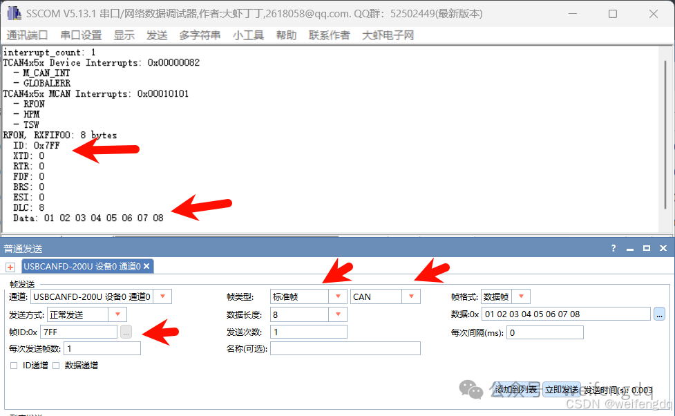
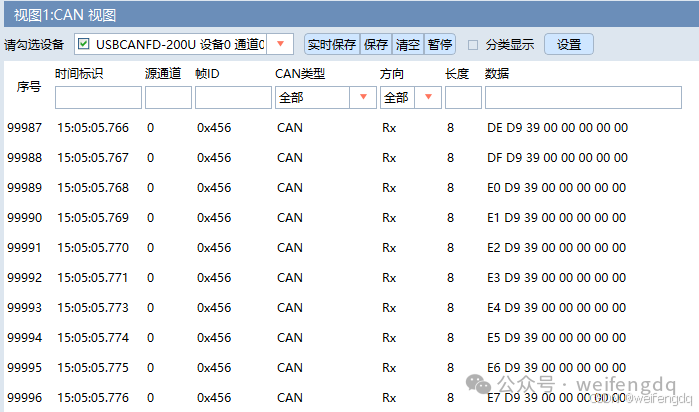
Below is a reading of a 12-byte CANFD extended frame:
RF0N, RXFIFO0: 12 bytes
  ID: 0x1234567A
  XTD: 1
  RTR: 0
  FDF: 1
  BRS: 1
  ESI: 0
  DLC: 9
  Data: 01 02 03 04 05 06 07 08 00 00 00 00
VCCOUT Direct 5V Test
Short-circuiting VSUP and VCCOUT to 5V can work normally, but 4.9V will not work, indicating that powering VSUP and VCCOUT directly from USB is risky.
Similarly, VSUP can work at 5.4V, but 5.3V will not work, indicating a 0.4V drop to VCCOUT.
In summary, ensure that VCCOUT is stable at 5V for operation.
Open Circuit, Short Circuit, and Busoff Test
Short circuits had no effect (no need to reinitialize):
- Short-circuiting CANL to ground seems to have no effect
- Short-circuiting CANH to VSUP has no effect (note that the CAN’s TVS is 24V, so VSUP should not exceed 24V during short circuit testing)
- Disconnecting CANH or CANL
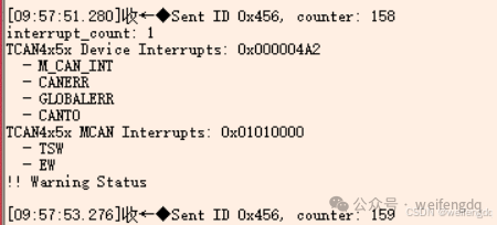
- Short-circuiting CANH and CANL momentarily triggers a warning but does not trigger Busoff; after unshorting, it can continue to work, as shown in the figure
Will trigger Busoff (the program has been continuously sending every 10ms), cannot automatically recover, requires reinitialization after 100ms:
- Short-circuiting CANL to VSUP
- Short-circuiting CANH to ground
- First disconnect CANH or CANL, then short-circuit CANH and CANL
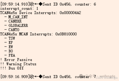
- Short-circuiting CANH and CANL for too long will trigger Busoff, as shown in the figure
Gradually lowering the VSUP voltage to below 5.4V causes the board to stop working, and raising it again will trigger the UVSUP interrupt. This interrupt can be enabled to capture the interrupt, and after capturing, reconfigure after 100ms to attempt to restore normal operation.
Program Link
github.com/weifengdq/embedded/tree/main/tcan4550
Environment:
- STM32CubeMX 6.14.0
- STM32Cube MCU Package for STM32G4 Series 1.6.1
The above link or blog.csdn.net/weifengdq/article/details/146324740 contains information on purchasing the modified board from the seafood market; interested parties can visit on their own.
Discussion Group
QQ Group: 1040239879