@[toc]
Impact of SPI Communication Modes on DMA Controller Configuration Strategies
1. Introduction
The Serial Peripheral Interface (SPI) is a synchronous, full-duplex serial communication protocol widely used in embedded systems for data exchange between microcontrollers and various peripherals (such as sensors, memory, and display controllers). Although its physical layer is defined as full-duplex, in practical applications, it can be categorized into various operational modes such as full-duplex, half-duplex, and three-wire simplex based on the data flow direction. Different operational modes impose distinctly different requirements on the underlying drivers, particularly the configuration strategies of the Direct Memory Access (DMA) controller. This article aims to deeply analyze the various communication modes of SPI and focus on why the combination of “Polling TX” and “DMA RX” is unfeasible in full-duplex mode, as well as how this configuration disrupts the protocol’s synchronization.
2. Core of the SPI Protocol: The Physical Basis of Synchronization and Full-Duplex
To understand the derivation of different modes, one must first grasp the fundamental mechanism of the SPI protocol.
2.1 Physical Connections
The standard four-wire SPI bus consists of the following signal lines:
- • SCLK (Serial Clock): The clock signal generated by the master device, synchronizing all data transfers on the bus.
- • MOSI (Master Out, Slave In): Data output from the master device, data input to the slave device.
- • MISO (Master In, Slave Out): Data input to the master device, data output from the slave device.
- • CS/SS (Chip Select / Slave Select): Chip select signal controlled by the master device to select the slave device for communication.
Slave Device
Master Device


SCLK
MOSI
MISO
CS
SCLK
MISO
MOSI
CS
2.2 Core Mechanism: Synchronous Data Exchange
The core of SPI transmission is a circular shift register model. For each SCLK clock cycle generated by the master device, a bidirectional data bit exchange occurs:
- 1. The master device pushes the most significant bit (MSB) of its transmit shift register onto the MOSI line.
- 2. The slave device simultaneously pushes the MSB of its transmit shift register onto the MISO line.
- 3. Within the same clock cycle, the master device captures the data bit on the MISO line and shifts it into the least significant bit (LSB) of its receive shift register.
- 4. The slave device captures the data bit on the MOSI line and shifts it into the LSB of its receive shift register. This process continues for N clock cycles (where N is the data frame length, typically 8 or 16), completing a full data exchange. The key point is that sending and receiving occur synchronously; sending one bit necessarily involves receiving one bit. This is the essence of the “full-duplex” nature of the SPI protocol at the physical layer.
Master Device


Slave Device


No

Yes

SCLK clock cycle N Start
Data exchange
Send 1 bit data to MOSI
Send 1 bit data to MISO
Receive 1 bit data from MISO
Receive 1 bit data from MOSI
Complete 1 bit exchange
Reached N clock cycles?
Transmission end
3. Classification of SPI Communication Modes
Based on the full-duplex characteristics of the physical layer, upper-layer applications can evolve various logical communication modes.
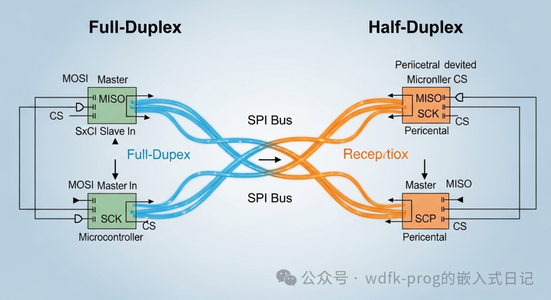
3.1 Full-Duplex Mode
In this mode, data on both the MOSI and MISO lines is valid at the same time. The master device sends data to the slave device while also receiving data sent back from the slave device.
- • Application Scenarios: Communication with ADC/DAC modules, other microcontrollers, or complex peripherals requiring synchronized command and status exchanges.
- • Data Flow:
<span>send_buf</span>and<span>recv_buf</span>both contain valid data.
Slave -> Master (MISO)
Master -> Slave (MOSI)
Timeline


Synchronous occurrence


Synchronous occurrence

Start
End
Send valid data
Receive valid data
3.2 Half-Duplex Mode
Although data exchange still occurs physically, logically only one direction of data is valid.
- • Write Operation (Transmit-Only): The master device sends data via MOSI but ignores any data received on MISO. At this time, the data on the MISO line is typically invalid or unimportant.
- • Read Operation (Receive-Only): The master device needs to read data from the slave device. To generate the necessary SCLK clock, the master device must send data via MOSI, but this data is meaningless “dummy data”. The master device only cares about the valid data received on the MISO line.
- • Application Scenarios: Reading and writing EEPROM/Flash memory, configuring simple sensors, etc.
Write Operation

Read Operation

Half-Duplex Mode
Operation Type?
MOSI: Valid Data MISO: Ignored
MOSI: Dummy Data MISO: Valid Data
3.3 Three-Wire Simplex Mode
This is a hardware simplification of half-duplex mode. In purely unidirectional communication scenarios (for example, when the master device only sends data to a display driver), the MISO line can be completely omitted, saving a GPIO pin.
- • Application Scenarios: Driving seven-segment displays, LED strips, and some simple screens.
Slave Device
Master Device


SCLK
MOSI
CS
SCLK
MOSI
CS
4. DMA Configuration Strategies and Inherent Conflicts in Full-Duplex Mode
Now, let us analyze why the combination of “Polling TX + DMA RX” has fundamental logical flaws in full-duplex mode.
4.1 Problem Statement
In a hypothetical SPI driver function, to handle full-duplex transmission, one might attempt the following mixed programming model:
- 1. Send: Use blocking (Polling) or interrupt-based methods to send data. The CPU loops waiting for the transmit buffer (TX FIFO) to be empty, then writes the next byte until all data is sent.
- 2. Receive: Simultaneously, configure a DMA channel for the receive path. The expectation is that DMA will automatically transfer data from the receive buffer (RX FIFO) to memory once the SPI hardware receives data.
Is

Start full-duplex transmission
CPU executes blocking send loop
Configure and start RX DMA channel
Send complete?
End
DMA waits for RXNE event
4.2 Root Cause of the Conflict: Disruption of Synchronization
The failure of this design stems from its erroneous decomposition of the SPI synchronous exchange process into two independent, asynchronous tasks, which the SPI hardware itself does not support.
- 1. Source of the Clock: The SCLK clock of SPI is generated by the master device’s data transmission. When the CPU writes data to the TX FIFO in a blocking manner, the SPI hardware begins the shifting operation and generates the clock.
- 2. Dependency of Reception: Data reception is entirely dependent on the SCLK clock. Without the clock, there is no data exchange, and the RX FIFO will never receive new data.
- 3. Logical Deadlock:
- •
<span>RX DMA</span>channel, once started, passively waits for the SPI hardware to issue a “new data received” (RXNE) request signal. - • However, the
<span>RXNE</span>signal is only generated when data is shifted into the receive register from the MISO line under the drive of the SCLK clock. - • The SCLK clock, in turn, depends on the transmission operation executed by the CPU.
- • If the CPU executes a complete blocking send function (for example,
<span>HAL_SPI_Transmit()</span><code><span>), it will send all data at once. During this process, all clocks are indeed generated, and data is received into the RX FIFO. However, when this send function returns, the DMA may not have had time to transfer all data, or worse, if the amount of received data is large, the RX FIFO may have already overflowed.</span> - • More fundamentally, a well-designed driver would not separate these two operations. It would call a unified full-duplex transmission function, such as
<span>HAL_SPI_TransmitReceive_DMA()</span><span>. This function would simultaneously configure TX DMA and RX DMA, ensuring that the initiation and data flow of sending and receiving are managed synchronously.</span>
4.3 A Clearer Failure Scenario
Imagine a driver attempting to implement <span>transmit_polling_receive_dma(tx_buf, rx_buf, len)</span>:
- 1. Configure RX DMA:
<span>HAL_SPI_Receive_DMA(&hspi, rx_buf, len);</span>This statement configures the DMA and enables the SPI receive interrupt/DMA request. The SPI hardware now begins waiting for data. - 2. Execute Blocking TX:
<span>HAL_SPI_Transmit(&hspi, tx_buf, len, timeout);</span>The CPU enters this function and begins looping to write data to the TX FIFO. - 3. Competition and Conflict:
- • The CPU writes the first byte to the TX FIFO, and the SPI hardware begins generating the clock.
- • The first byte of data exchange occurs, one byte is received into the RX FIFO, triggering the RX DMA request, and DMA begins transferring data.
- • The CPU may continue to fill the TX FIFO at a very high speed, while DMA transfer takes time. If the CPU’s sending speed exceeds the DMA’s ability to process received data, the
<span>RX FIFO</span>will overflow, leading to data loss. - • This separated calling method completely disrupts the atomic operation designed in the HAL library, making state management and error handling during the transmission process unreliable.
DMASPI_HardwareCPUDMASPI_HardwareCPURX FIFO overflow (Overrun) Configure and start RX DMA Enable RXNE request Start blocking send first byte (HAL_SPI_Transmit) Generate clock, exchange data Trigger RXNE, request transfer Immediately send second byte (CPU speed >> DMA) (Processing first byte) Generate clock, exchange data Trigger RXNE, but DMA may still be processing the previous request5. Conclusion
The physical layer of the SPI protocol is inherently full-duplex and synchronous, tightly coupling data sending and receiving operations under the drive of the clock. Although upper-layer applications can implement various modes such as full-duplex and half-duplex based on logical needs, the implementation of the underlying driver must strictly respect its synchronization.
Decomposing full-duplex transmission into “blocking send” and “DMA receive” as two independent tasks is unfeasible because it:
- 1. Disrupts Synchronization: Incorrectly decouples the reception process driven by the sending behavior.
- 2. Introduces Race Conditions: There is competition between the CPU’s sending speed and the DMA’s receiving processing speed, which can easily lead to RX FIFO overflow and data loss.
- 3. Violates the Atomicity of Driver Design: A reliable SPI driver must manage full-duplex transmission atomically through a unified interface (such as
<span>HAL_SPI_TransmitReceive_DMA()</span><span>), ensuring that the TX and RX DMA channels are synchronously configured and started, thereby maintaining the integrity of the protocol and the consistency of the data.</span>
Therefore, when designing SPI drivers, it is essential to select the correct and matching transmission strategy based on the communication mode to avoid introducing such fundamental logical contradictions.