
Introduction
The temporary lifting of EDA tool restrictions does not equate to technical security.
Download for free today: 2025 Third Generation Semiconductor Industry Chain Research Report
Source: Semiconductor Industry Overview
Author: Feng Ning
Since the issuance of the EDA ban, the market has exploded.
Recently, this ban has released new signals.
01EDA Giants Lift Export Ban
On July 2, U.S. time, Siemens announced that it had received notification from the U.S. government that restrictions on the export of chip design software to mainland China had been lifted. According to the company’s statement, it has resumed providing its software and technical services to Chinese customers.
At the same time, Synopsys and Cadence have also received notifications lifting export restrictions to China.
This lifting of the ban comes just two months after the ban was issued.
On May 29, 2025, the U.S. Department of Commerce’s Bureau of Industry and Security (BIS) issued a ban requiring the three major EDA giants to completely stop providing chip design software to China. The core goal of this control is to strictly regulate chip development and design related to artificial intelligence and further strengthen controls over so-called entity list companies.
In the global EDA market, U.S. companies hold a monopoly position. According to TrendForce data, by 2024, Synopsys, Cadence, and Siemens EDA will occupy 32%, 29%, and 13% of the global EDA market share, respectively, totaling 74%. In the domestic EDA market, these three giants hold over 80% market share.
Since 2018, the U.S. has initiated multiple rounds of restrictions on EDA tools.
In 2019 and 2020, the U.S. listed several leading Chinese semiconductor/technology companies on the entity list, restricting their access to high-end EDA software.
In 2022, the U.S. Department of Commerce revised the Export Administration Regulations (EAR) to add export control classification number ECCN 3D006, specifically targeting EDA tools that can be used to design GAAFET (Gate-All-Around Field Effect Transistor) structures, primarily used for 3nm and below chip designs.
In the context of domestic EDA software being highly reliant on imports, the inability to access relevant tools will directly impact the technological research and development process.
02How Important is EDA?
What makes EDA so important?
The author summarizes it as: high technical difficulty + monopoly and deep binding.
EDA, or Electronic Design Automation, is also known as the “mother of chips.” It includes a series of software tools from design to manufacturing, covering functional design, wiring, verification, etc., and is an indispensable component in chip design.
In front-end design, as chip designs become increasingly complex, the cost of tape-out is also rising. It is reported that the cost of tape-out for the lowest-end chips exceeds hundreds of thousands, while advanced processes can even exceed hundreds of millions, making it difficult for small and medium-sized chip companies to bear the cost of multiple tape-outs. Therefore, chip design needs to pursue a high success rate, and automated design tools can greatly avoid circuit design and layout errors, reducing losses.
Thus, EDA is crucial in chip design.
In the chip manufacturing process, international EDA leaders also form a monopoly over chip design companies.
In simple terms, the integrated circuit industry has undergone a long period of division and integration, with various links in the industry chain having a “mutual adaptation” binding relationship.
From upstream instruction set architecture, EDA tools, to manufacturing photolithography machines, etching machines, and even backend packaging and testing equipment, the research and improvement of each link require cooperation and mutual adaptation between upstream and downstream links.
For example, in TSMC’s technology updates, users often see the term PDK. PDK stands for Process Design Kit, which can be understood as a user manual for a certain node of the foundry, including design rules, simulation models, technical documents, and other design parameters for that node.
This also means that if downstream chip design companies want to design chips, they need to obtain development data packages (PDK) from foundries like TSMC, which include authorization verification for EDA software. Without authorization verification, EDA software cannot use the PDK toolkit.
Moreover, not all process nodes have the same PDK. For instance, TSMC has released four versions of PDK for its 3nm process to date: N3B, N3E, N3P, and N3X, each corresponding to different PDKs.
Through this method, leading EDA companies are deeply bound to chip design companies, forcing these companies to timely update their EDA tools.
The Chinese EDA industry began in the 1980s, with the birth of the domestic integrated circuit computer-aided design system “Panda System” in 1986 marking the start of the industry. However, due to the weak foundation of the domestic semiconductor industry and insufficient R&D investment at that time, the development of domestic EDA has been slow, and the market has long been monopolized by international giants.
Currently, there is still a significant gap between domestic EDA and international EDA leaders.
03What Challenges Does Domestic EDA Face?
For EDA companies, the higher the integration level, the more advantageous it is. However, a complete set of EDA tools is extremely complex.
EDA tools can be divided into three categories: digital chip design full-process EDA, analog and mixed-signal circuit design full-process EDA, and integrated circuit manufacturing EDA.
Among them, digital circuit design full-process tools can be divided into front-end and back-end parts based on the design process, with different design tools and verification tools for each; analog and mixed-signal circuit design tools focus on circuit design, simulation verification, and physical implementation; while integrated circuit manufacturing EDA tools are used to develop manufacturing process platforms and wafer manufacturing.
All three major EDA giants can provide full-process EDA tool solutions.
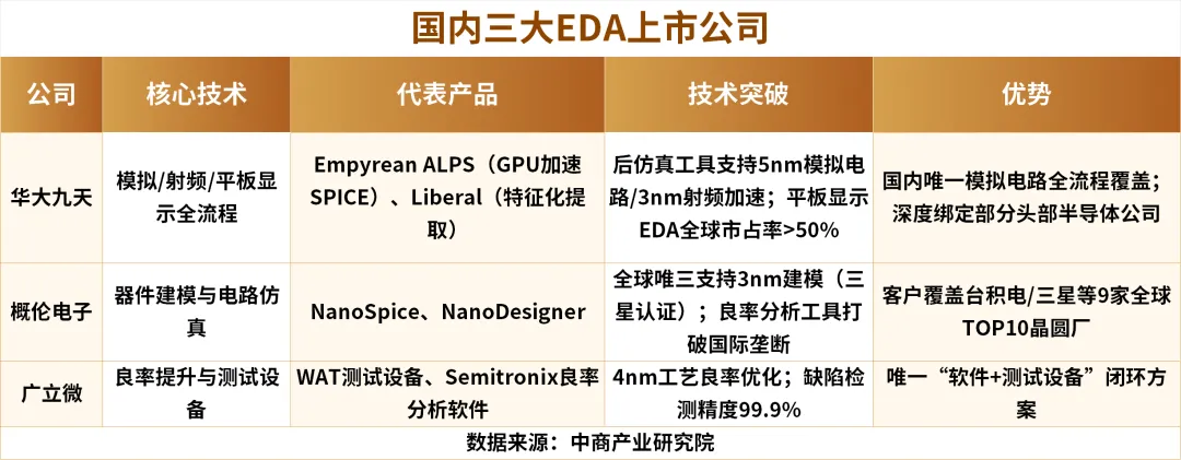
In recent years, domestic EDA companies represented by Huada Jiutian, Gailun Electronics, and Guangli Micro have gradually established a foothold in the market by focusing on niche areas and differentiated competition strategies.
Huada Jiutian focuses on digital circuit design, with a relatively complete digital EDA solution for front-end and some back-end; Gailun Electronics specializes in analog circuit design EDA solutions; Guangli Micro focuses on EDA verification tools. Currently, none of the three major manufacturers have independent full-process EDA toolchain capabilities. Overall, using a combination of multiple domestic EDA point tools can theoretically cover the full process, but capabilities in certain areas are relatively weak.
Other important participants in EDA tools include Xinheng Semiconductor and Xinhua Zhang.
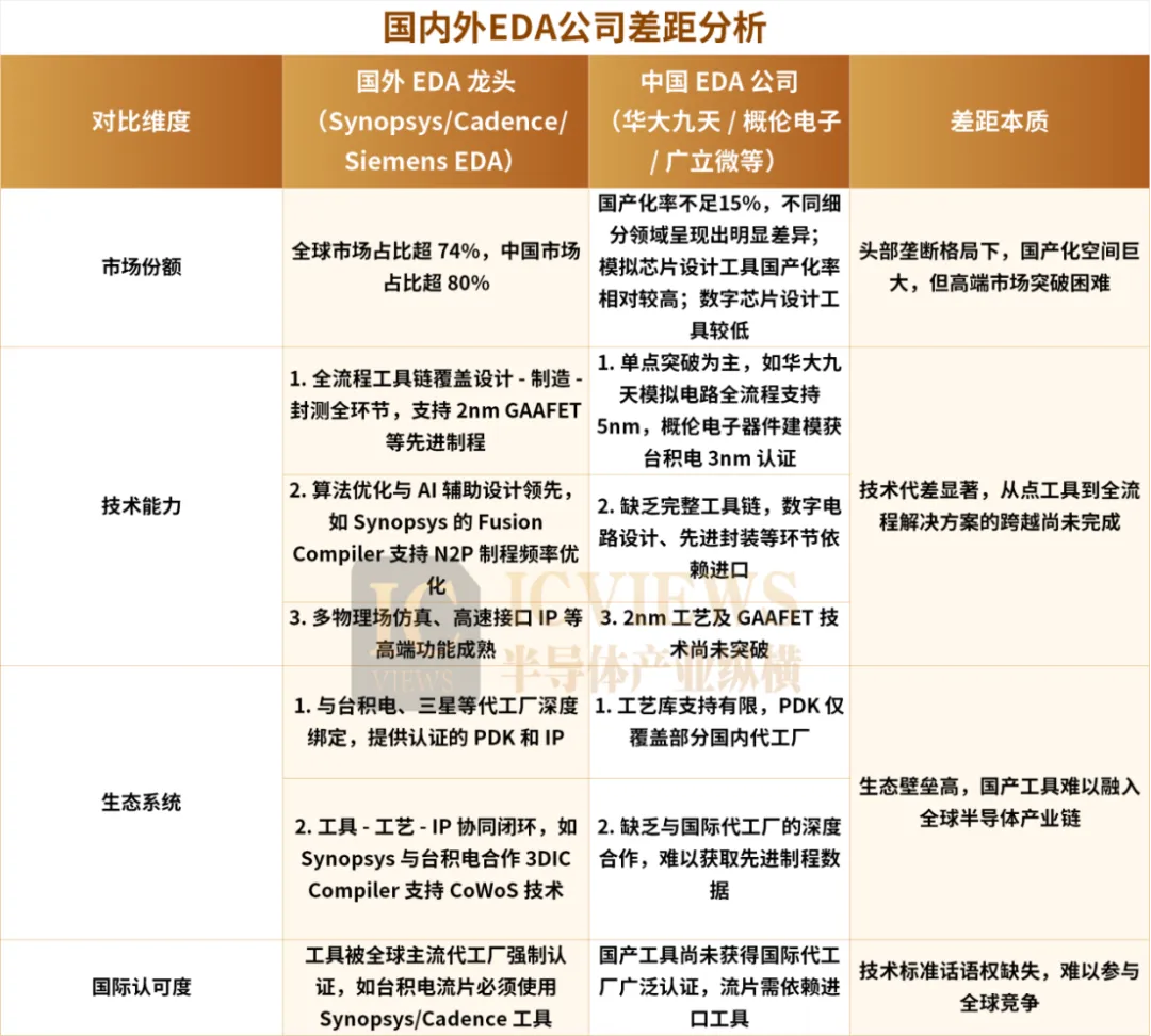
Domestic EDA companies have significant gaps with international giants in advanced process support and toolchain integrity, especially in cutting-edge fields such as processes below 3nm and multi-physical field simulation.In terms of ecology, as mentioned above, EDA, being a tool software that highly relies on upstream and downstream collaboration, needs to establish a close PDK (Process Design Kit) adaptation relationship with foundries and design companies. The three international giants have established decades-long collaborations with leading foundries like TSMC and Samsung, forming extremely high ecological barriers.
However, this situation is undergoing positive changes: on one hand, the U.S. export control of high-end EDA tools to China is forcing downstream companies to increase the verification and introduction of domestic software, and some semiconductor leaders have actively begun to build a local EDA ecosystem; on the other hand, local companies are gradually advancing into “deep waters” such as full-process digital design and high-end process support through technological innovation and strategic acquisitions.
Technologically, domestic EDA companies are not only strengthening independent R&D but also accelerating the pace of acquisitions, such as Huada Jiutian acquiring Xinheng Semiconductor to fill the gap in RF design tools. In terms of ecological reconstruction, in addition to state-guided ecological collaboration, domestic manufacturers are actively participating in the RISC-V open-source ecosystem, promoting the standardization of domestic EDA tool interfaces to reduce dependence on U.S. tools.
Gailun Electronics has also made a significant acquisition worth billions—fully acquiring Ruicheng Semiconductor (with a 15% market share in semiconductor IP) through stock issuance and cash payment, and holding Naneng Micro.
Gailun Electronics’ main products are full-process solutions for design and manufacturing EDA, with leading advantages in analog, storage, RF, flat panel display, and digital circuit fields.
By acquiring Ruicheng Semiconductor, Gailun Electronics has completed its IP layout in analog, mixed-signal, storage, RF, and interface fields, which is expected to achieve technological and customer synergy, enhancing the company’s product development and customer expansion efficiency in the EDA and IP fields, helping the company become a leading EDA+IP platform enterprise.
So, what impact will the lifting of the export ban have on China’s semiconductor industry?
04Impact of Lifting EDA Export ControlFrom a positive perspective, for China’s semiconductor industry, regaining access to international advanced EDA technology and products will help companies enhance chip design capabilities and efficiency, accelerate the R&D process of high-end chips, narrow the gap with international advanced levels, and promote the high-quality development of the domestic semiconductor industry.
From a negative perspective, while imported EDA technology is indeed advanced, what if the supply interruption occurs again? It is important to note that the temporary lifting of EDA tool restrictions does not equate to technical security. The U.S. Department of Commerce retains the right to adjust policies, and the limitations of the current lifting cannot be ignored.
What might the situation look like after the lifting of the ban?
From the short-term operation of the industry, domestic semiconductor companies will quickly restart cooperation with international EDA giants, high-end chip design projects will be restored, and some advanced process R&D is expected to accelerate. However, this may also exacerbate dependence on imported tools, as companies become accustomed to using mature and efficient international EDA tools, which may weaken the motivation to explore domestic solutions.
Previously, after the U.S. suddenly cut off EDA software supply, several domestic EDA manufacturers such as HJSoft, Xinhua Zhang, and Jiutongfang announced free trial offers.
If the three international EDA giants regain market dominance, it may squeeze the survival space of domestic manufacturers. In this regard, domestic semiconductor companies need to have a sense of crisis.
Achieving the localization of EDA software is of utmost importance.
To truly break free from technological dependence and achieve industrial security, accelerating the independent process of domestic EDA equipment is key.
This also means that achieving the autonomy of the EDA tool library requires not only leading companies like Huada Jiutian to increase R&D investment and continuously tackle core issues in algorithm optimization and toolchain integration but also relies on domestic semiconductor companies providing more practical opportunities for domestic tools, promoting technological iteration and upgrades through feedback from actual application scenarios.
Only by forming a virtuous cycle of “R&D—Application—Improvement” can we gradually build a self-controllable EDA industry ecosystem, fundamentally enhancing the risk resistance capability of China’s semiconductor industry.
Recommended Reading:1. Detailed Explanation of the Photolithography Machine Industry Chain2. Overview of the Computing Power-Related Industry Chain3. Comprehensive Overview of the A-Share Automotive Industry Chain4. Analysis of the Domestic Collection Industry5. Ranking of China’s Unicorn Enterprises
——END——
[PS: Click for details to view content]

Click the WeChat mini-program 👉: “Report Search”; Download various industry research reports in PDF and Word, visual data, and learning materials. Provides research reports, market research reports, industry reports, industry research reports, survey reports, market investigation reports…