
1. Basic Concept of Reflow
In the schematic of digital circuits, the propagation of digital signals occurs from one logic gate to another, with signals traveling through wires from the output to the receiving end, appearing to flow in a unidirectional manner. Many digital engineers thus believe that the return path is irrelevant, as both drivers and receivers are specified as voltage mode devices. However, basic circuit theory tells us that signals propagate through current, specifically through the movement of electrons. One characteristic of electron flow is that electrons never stay anywhere; wherever the current flows, it must return. Therefore, current always flows in a loop, and any signal in a circuit exists in the form of a closed loop. For high-frequency signal transmission, it is essentially the process of charging the dielectric capacitance sandwiched between the transmission line and the DC layer.
 2. Impact of ReflowDigital circuits typically complete reflow through ground and power planes. The return paths for high-frequency and low-frequency signals differ; low-frequency signals choose the path of least impedance, while high-frequency signals select the path of least inductive reactance. When current flows from the signal driver through the signal line to the receiving end, there is always a return current flowing in the opposite direction: starting from the ground pin of the load, passing through the copper plane, and returning to the signal source, forming a closed loop with the current flowing through the signal line. The noise frequency caused by the current flowing through the copper plane is comparable to the signal frequency; the higher the signal frequency, the higher the noise frequency. Logic gates do not respond to absolute input signals but to the difference between the input signal and the reference pin. Single-ended circuits respond to the difference between the incoming signal and its logical ground reference plane, making disturbances on the ground reference plane and interference on the signal path equally important. Logic gates respond to the input pin and the specified reference pin, but it is unclear which is the designated reference pin (for TTL, it is usually the negative power supply, while for ECL, it is typically the positive power supply, but this is not always the case). In this regard, the anti-interference capability of differential signals can effectively mitigate ground bounce noise and power plane sliding.When numerous digital signals on a PCB switch synchronously (such as the CPU’s data bus, address bus, etc.), it causes transient load currents to flow from the power supply into the circuit or from the circuit into the ground. Due to the impedance present on the power and ground lines, synchronous switching noise (SSN) is generated, and ground bounce noise (referred to as ground bounce) also appears on the ground line. The larger the area surrounded by the power and ground lines on the printed circuit board, the greater their radiated energy. Therefore, we analyze the switching states of digital chips and take measures to control the reflow method to minimize the surrounding area and reduce radiation levels.Example Explanation:
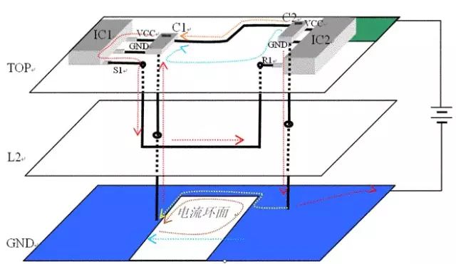 IC1 is the signal output end, and IC2 is the signal input end (for simplification of the PCB model, it is assumed that the receiving end contains a pull-down resistor). The third layer is the ground layer. The grounds of IC1 and IC2 both come from the third layer ground plane. The top layer’s upper right corner is a power plane connected to the positive power supply. C1 and C2 are the decoupling capacitors for IC1 and IC2, respectively. The power and ground pins of the chips shown in the diagram are the power and ground for the signal transmission.At low frequencies, if the S1 end outputs a high level, the entire current loop is from the power supply through the wire to the VCC power plane, then entering IC1 via the orange path, exiting from the S1 end, and entering IC2 through the wire on the second layer at the R1 end, then entering the GND layer, returning to the negative power supply via the red path.At high frequencies, the distributed characteristics presented by the PCB have a significant impact on the signal. The so-called ground reflow is a common issue encountered with high-frequency signals. When there is an increased current in the signal line from S1 to R1, the rapidly changing external magnetic field induces a reverse current in nearby conductors. If the third layer ground plane is complete, a current indicated by the blue dashed line will be generated on the ground plane. If the top layer has a complete power plane, there will also be a return flow along the blue dashed line on the top layer. At this point, the signal loop has the smallest current loop, minimizing the energy radiated outward and the ability to couple external signals (the skin effect at high frequencies also minimizes outward radiated energy, and the principle is the same).Since high-frequency signal levels and current changes are rapid, but the change period is short, the energy required is not very large. Therefore, the chip draws power from the nearest decoupling capacitor. When C1 is sufficiently large and responds quickly (with a very low ESR value, typically using ceramic capacitors, which have an ESR far lower than tantalum capacitors), the orange path on the top layer and the red path on the GND layer can be considered non-existent (there is a current corresponding to the overall board power supply, but not the current corresponding to the signal shown in the diagram).Thus, in the environment constructed in the diagram, the entire current path is: from the positive terminal of C1 → VCC of IC1 → S1 → L2 signal line → R1 → GND of IC2 → via hole → yellow path on the GND layer → via hole → negative terminal of the capacitor. It can be seen that there is an equivalent current in the vertical direction, which induces a magnetic field in the middle, and this loop can easily couple to external interference. If the signal in the diagram is a clock signal, and there is a parallel set of 8-bit data lines powered by the same chip’s power supply, the current return path is the same. If the data line levels flip simultaneously in the same direction, it will induce a large reverse current on the clock, and if the clock line is not well matched, this crosstalk can have a fatal impact on the clock signal. The strength of this crosstalk is not proportional to the absolute value of the high and low levels of the interference source, but rather proportional to the rate of change of the interference source’s current. For a purely resistive load, the crosstalk current is proportional to dI/dt = dV /(T¬10%-90%*R). In this formula, dI/dt (current change rate), dV (interference source swing), and R (interference source load) all refer to the parameters of the interference source (if it is a capacitive load, dI/dt is inversely proportional to the square of T¬10%-90%). From this formula, it can be seen that low-frequency signals are not necessarily less crosstalk-prone than high-speed signals. This is what we mean when we say: a 1KHz signal is not necessarily a low-speed signal; the situation must be considered comprehensively. For signals with steep edges, they contain many harmonic components, with significant amplitudes at all harmonic frequencies. Therefore, when selecting devices, care should be taken not to choose chips solely based on fast switching speeds, as this not only increases costs but also exacerbates crosstalk and EMC issues.Any adjacent power layer or other plane can serve as the return plane for a signal as long as there are suitable capacitors at both ends of the signal providing a low reactance path to GND. In typical applications, the power supply for the corresponding chip IO is often the same, and there is generally a 0.01-0.1uF decoupling capacitor between their respective power and ground, which happens to be at both ends of the signal. Therefore, the return effect of this power plane is second only to that of the ground plane. However, when borrowing other power planes for return, there often isn’t a low reactance path to ground at both ends of the signal. In this case, the current induced in the adjacent plane will seek the nearest capacitor to return to ground. If this “nearest capacitor” is far from the starting or ending point, this return will have to traverse a “long journey” to form a complete return path, and this path is also the return path for adjacent signals, which has the same effect as common ground interference, effectively resulting in crosstalk between signals.For some unavoidable cases of crossing power splits, capacitors or RC series high-pass filters (such as a 10-ohm resistor in series with a 680pF capacitor, specific values depend on the type of signal) can be placed at the split to provide a high-frequency return path while isolating low-frequency crosstalk between planes. This may involve adding capacitors between power planes, which seems a bit absurd but is definitely effective. If some specifications do not allow this, capacitors can be connected to ground at the split between the two planes.For cases where other planes are borrowed for return, it is best to add a few small capacitors to ground at both ends of the signal to provide a return path. However, this practice is often difficult to implement, as the surface area near the terminal is mostly occupied by matching resistors and the chip’s decoupling capacitors.Return noise is one of the main sources of noise on the reference plane. Therefore, it is necessary to study the path and flow range of the return current.3. Theoretical Knowledge of Return PathsThe following diagram shows a line on a printed circuit board with current flowing through the conductor. Typically, we only see the surface-mounted wires used for signal transmission from the driver to the receiver. In reality, current can only flow in a loop, and while the transmission line is visible, the return path of the current is usually invisible. They typically flow back through the ground plane and power plane. Due to the lack of physical lines, estimating the return path becomes challenging, and controlling them is somewhat difficult.As shown in Figure 3.1, each wire on the PCB and its loop forms a current loop. According to the principles of electromagnetic radiation, when a sudden current flows through the wire loop in the circuit, it generates an electromagnetic field in space, affecting other wires. This is what we commonly refer to as radiation. To reduce the impact of radiation, it is essential to understand the basic principles of radiation and the parameters related to radiation intensity.
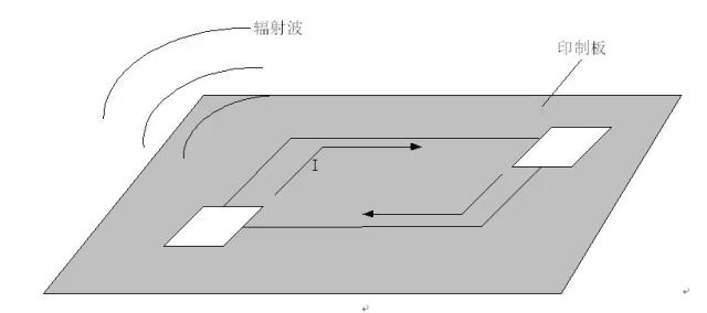 Figure 3.1 Differential Mode Radiation on the Printed Circuit BoardThese loops act like small antennas in operation, radiating magnetic fields into space. We simulate the radiation produced by a small loop antenna, assuming a current of I and an area of S for the small loop, the electric field strength measured in the far field at a distance r in free space is:
 E――Electric Field (V/m)f――Frequency ( )S――Area ( )I――Current (A)r――Distance (m)――Angle between the measuring antenna and the radiation plane ( )Equation 3.1 applies to a small loop placed in free space with no surface reflections. In reality, our products are grounded rather than in free space, and nearby ground reflections can increase the measured radiation by 6dB. Considering this, Equation 3.1 must be multiplied by 2. If we correct for ground reflections and assume the maximum radiation direction, Equation 3.1 becomes:
 From Equation 3.2, it is known that radiation is proportional to the loop current and the loop area, and is proportional to the square of the current frequency.The return current path in a printed circuit board is closely related to the frequency of the current. According to basic circuit knowledge, DC or low-frequency currents always flow in the direction of least impedance; while high-frequency currents, under constant resistance, always flow in the direction of least inductive reactance.If we disregard the effects of holes and grooves formed by vias on the copper plane, the path of least impedance, which is the path for low-frequency currents, consists of arc lines on the ground copper plane, as shown in Figure 3.2. The current density on each arc line is related to the resistivity of that arc line.
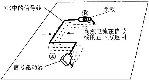 Figure 3.2 High-Frequency Current Path on PCB Copper PlaneFor transmission lines, the path of least inductive reactance for return, which is the return path for high-frequency currents, lies directly beneath the signal routing on the copper plane, as shown in Figure 3.3. This return path minimizes the area enclosed by the entire loop, thereby minimizing the magnetic field strength radiated by this signal (or the ability to receive space radiation).For longer, straight wiring, it can be considered an ideal transmission line. The range through which the return current flows is a banded area centered on the signal routing, with the current density decreasing as the distance from the center axis of the signal routing increases, as shown in Figure 3.3. This relationship approximately satisfies Equation 3.3 [4]:
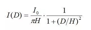 Equation 3.3Where, is the original signal current, measured in “A, Amperes”; is the distance from the signal routing to the copper plane, measured in “in., inches”; is the vertical distance from the point on the copper plane to the signal line, measured in “in., inches”; is the current density at this point, measured in “A/in., Amperes per inch”.
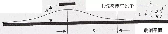 Figure 3.3 Distribution of Return Current Density in Transmission LineAccording to Equation 3.3, Table 3.1 lists the percentage of return current flowing through a banded area centered on the transmission line with a width of .
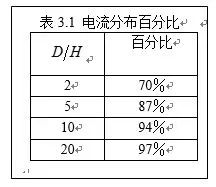 Assuming inches, the return current flowing beyond 0.035 inches from the transmission line only accounts for 13% of all return current, with only 6.5% distributed to one side of the transmission line, and the density is very low. Therefore, it can be neglected.Summary:1. When there is a continuous, dense, and complete copper plane beneath the signal routing, the noise interference of the signal return current on the copper plane is localized. Therefore, as long as the principles of layout and localized routing are followed, i.e., artificially increasing the distance between digital signal lines, digital devices, and analog signal lines, analog devices to a certain extent, the interference of digital signal return currents on analog circuits can be significantly reduced.2. High-frequency transient return currents flow back to the driver end via the plane adjacent to the signal routing (ground plane or power plane). The load at the driver signal routing is bridged between the signal routing and the plane adjacent to the signal routing (ground plane or power plane).3. The larger the area surrounded by the power and ground lines on the printed circuit board, the greater their radiated energy. Therefore, by controlling the return path, we can minimize the surrounding area and control the radiation level.4. Solutions to Return Path IssuesReturn path issues on PCBs typically arise from three aspects: chip interconnections, copper plane cuts, and via jumps. Below, we analyze these factors in detail.4.1 Return Path Issues Caused by Chip InterconnectionsWhen digital circuits operate, transitions between high and low voltages occur, causing transient load currents to flow from the power supply into the circuit or from the circuit into the ground.For digital devices, their pin input resistance can be considered infinite, equivalent to an open circuit (i.e., i=0 in the diagram below). In reality, the return loop current flows back through the distributed capacitance and inductance generated between the chip and the power and ground planes. The following analysis uses a collector output circuit as an example of the internal circuit for output signals.4.1.1 When the driver end changes from low to high level. When the output signal jumps from low to high level, it is equivalent to the output pin supplying a current to the transmission line. Since the input resistance is infinite, we consider that no current flows into the input pin of the chip, i.e., this current must return to the power pin of the output chip.① The signal routing is adjacent to the power plane.The driver charges the transmission line formed by the signal routing, power plane, and terminal load, with current flowing from the driver’s power pin into the device and from the driver’s output to the load end; high-frequency transient return current flows back to the driver’s output end via the power plane beneath the signal routing, forming a current loop.② The signal routing is adjacent to the ground plane.The driver charges the transmission line formed by the signal routing, power plane, and terminal load, with current flowing from the driver’s power pin into the device and from the driver’s output to the load end; high-frequency transient return current flows back to the driver’s output end via the ground plane beneath the signal routing, and the return current must cross from the ground plane to the power plane through the coupling capacitance at the driver’s output end, then enter the driver from the driver’s power pin, forming a current loop.4.1.2 When the driver end changes from high to low level, it is equivalent to the output pin absorbing current from the transmission line.① The signal routing is adjacent to the power plane.The load discharges the transmission line formed by the signal routing, power plane, and driver output end, with current flowing from the driver’s output pin into the device, exiting from the driver’s ground pin, entering the ground plane, and crossing to the power plane through the coupling capacitance near the driver’s ground pin, returning to the load end; high-frequency transient return current flows back to the load end via the power plane beneath the signal routing, forming a current loop.② The signal routing is adjacent to the ground plane.The load discharges the transmission line formed by the signal routing, power plane, and driver output end, with current flowing from the driver’s output pin into the device, exiting from the driver’s ground pin, entering the ground plane, and returning to the load end; high-frequency transient return current flows back to the load end via the ground plane beneath the signal routing, forming a current loop.
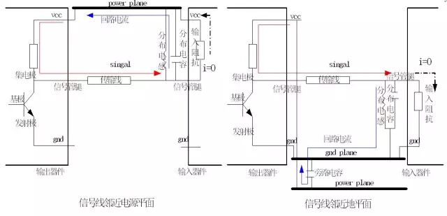 Near the driver’s output pin and ground pin, power plane and ground plane coupling capacitors should be placed to provide a return path for the return current; otherwise, the return current will seek the nearest coupling path between the power plane and ground plane (making the return path unpredictable and uncontrollable, thus causing crosstalk with other routing).4.2 Solutions to Return Path Issues Caused by Copper Plane CutsGround planes and power planes can reduce voltage loss caused by resistance. As shown, when the loop current flows back through the ground, the presence of resistance R1 inevitably causes a voltage drop at points 1 and 2. The greater the resistance, the larger the voltage drop, leading to inconsistencies in ground levels. If there is a ground layer, it can be viewed as a signal line with infinite width and very low resistance. The loop current always flows through the ground layer closest to the signal. When there are multiple ground layers, if the signal is between two identical ground planes, the loop current will be evenly distributed across both planes.
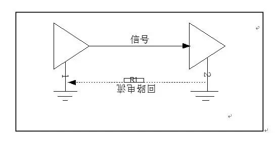 4.2.1. Under the conditions of layout and localized routing, the digital ground plane and analog ground plane share the same copper plane, meaning no distinction is made between digital and analog grounds. The noise from the digital circuit itself does not introduce additional noise to the analog circuit system.4.2.2. In mixed-signal systems, the common ground point for digital and analog grounds is chosen outside the board, meaning the two copper planes are completely independent, resulting in the signal lines between digital and analog circuits lacking transmission line characteristics, leading to severe signal integrity issues. Digital circuits and analog circuits use the same power system, with no ground plane segmentation. In the design of mixed-signal systems, based on modular layout and localized routing, the digital circuit module and analog circuit module share a complete, unsegmented voltage reference plane, which not only does not increase the interference of digital circuits on analog circuits but also significantly reduces crosstalk between signals and ground bounce noise, improving the accuracy of front-end analog circuits.
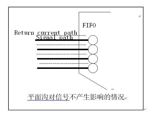
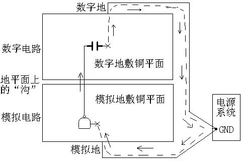 4.3 Solutions to Return Path Issues Caused by ViasWhen routing signals on printed circuit boards, especially multilayer boards, many signals must connect through layer changes, requiring a large number of vias. Vias can impact return paths in two ways: one is that vias form grooves that block return flow, and the other is that vias cause return flow to jump layers.4.3.1. Grooves Formed by ViasWhen routing signals on printed circuit boards, especially multilayer boards, many signals must connect through layer changes, requiring a large number of vias. If vias are densely arranged in the power or ground plane, they can sometimes form a series of connected vias, creating what is known as a groove, as shown in the diagram. First, we should analyze this situation to see if the return flow needs to pass through the groove. If the return of the signal does not require passing through the groove, it will not obstruct the return flow. If the loop circuit must bypass this groove to return, the resulting antenna effect will sharply increase, causing interference to surrounding signals. Typically, we can adjust the areas where vias are too dense and form grooves after the data generation is coated, leaving a certain distance between the vias.
 4.3.2. Layer Jump Phenomenon Caused by ViasNext, we analyze a six-layer board as an example. This six-layer board has two coated layers, with the second layer being the ground layer and the fifth layer being the power layer. Therefore, the signal return on the top layer and the third layer mainly occurs in the ground layer; the return on the bottom layer and the fourth layer mainly occurs in the power layer. There are six possible routing scenarios when changing layers: top layer <—–> third layer, top layer <—–> fourth layer, top layer <—–> bottom layer, third layer <—–> fourth layer, third layer <—–> bottom layer, fourth layer <—–> bottom layer. These six scenarios can be divided into two main categories based on the behavior of the loop current: whether the loop current flows on the same layer or on different layers, i.e., whether there is a layer jump phenomenon.A. Cases where loop current flows on the same layer include top layer <—–> third layer and fourth layer <—–> bottom layer, as shown in the diagram. In these cases, the loop current flows on the same layer, but according to the principle of electrostatic induction, a complete conductor in an electric field has zero internal electric field strength, and all current flows on the surface of the conductor. The ground plane and power plane effectively act as such a conductor. The vias we use are through vias, and the holes left by these vias when passing through the power and ground planes provide a path for current to flow between the upper and lower surfaces of the coated layer. Therefore, the return paths for these signal lines are good, and no measures are needed to improve them.B. Cases where loop current flows on different layers include top layer <—–> fourth layer, top layer <—–> bottom layer, third layer <—–> fourth layer, and third layer <—–> bottom layer. Below, we analyze the return situation for the top layer <—–> bottom layer and third layer <—–> fourth layer as examples. Signals with layer jump phenomena require additional bypass capacitors, typically 0.1uF ceramic capacitors, to be added near the area of dense vias to provide a return path.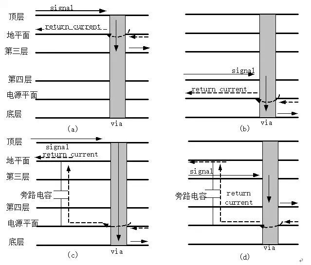


【Complete Set of Hardware Learning Materials】