This is a short paper. It is not recommended to do this in practice, but it is theoretically acceptable. The reason is that the dynamic range is not 1+1=2, but rather <2. Moreover, in 2025, the performance of devices has improved significantly; the simpler, the better. Complex signal chains do not provide much performance improvement and are not cost-effective!
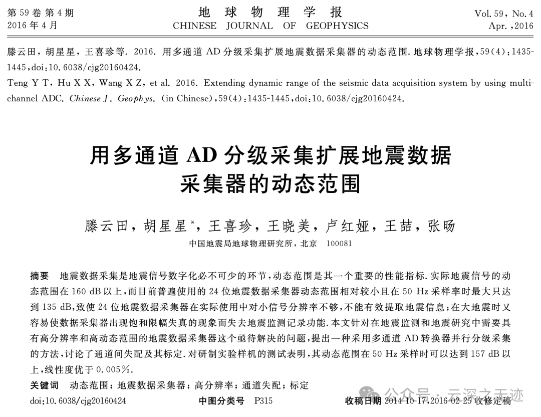 The dynamic range of seismic signals exceeds 160 dB, but traditional 24-bit ΣΔ ADCs have a dynamic range of only 135 dB at a 50 Hz sampling rate. → The resolution for small signals is insufficient (unable to extract weak information), and during large earthquakes, it is prone to saturation distortion, leading to the loss of critical observational data. Using multi-channel ADCs for hierarchical acquisition can extend the dynamic range of seismic data collectors; the goal is to design a high-resolution + high dynamic range data acquisition system, avoiding the cumbersome method of parallel dual devices (high gain/wide range acquisition).
Method
The core idea is to use multi-channel ADCs for hierarchical acquisition:
The same input signal → is sent to multiple ADC channels, but each channel has a different input range.
Small signal channel: pre-amplification to improve resolution;
Large signal channel: resistor network attenuation or level shifting to prevent saturation.
Ultimately, the CPU + digital switch (MUX) dynamically selects the appropriate channel to output the fitted 32-bit digital signal to extend the dynamic range of the seismic data collector using multi-channel ADC hierarchical acquisition.
Noise and Dynamic Range Analysis
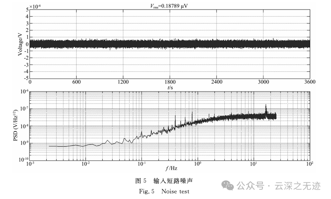
Modeling the noise of the preamplifier: input voltage noise + input current noise + resistor thermal noise → calculate the equivalent input noise to be approximately 25.7 nV_RMS.
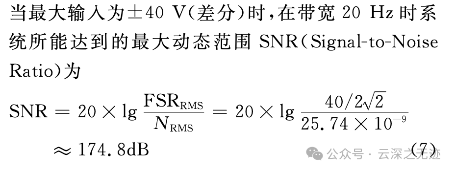
When the maximum input is ±40 V, the theoretical maximum dynamic range can reach 174.8 dB, but in practice, it will be limited by power supply noise, PCB leakage current, EMI, etc., using multi-channel ADC hierarchical acquisition to extend the dynamic range of the seismic data collector.
Prototype Design
ADC Selection: TI ADS1255 (24-bit, built-in PGA, ΣΔ modulator, excellent linearity ±0.001%).
Channel Configuration:
Small signal channel: PGA ×64, equivalent noise 0.122 μV; large signal channel: resistor network attenuation, input range extended to ±40 V.
Calibration and Error Control
Main Errors: “Crossover mismatch” between channels; offset mismatch (zero error); gain mismatch (voltage sensitivity differences).
Using precision resistors and low-noise amplifiers;
Derivation Symbols
: Equivalent noise bandwidth;
: Integral lower/upper limit frequency;
: Channel voltage gain (e.g., PGA multiple for small signal channel);
: Device white noise density (V/√Hz, A/√Hz);
: Device noise density normalized at 1 Hz;
: Front-end network resistance;
: Boltzmann constant, : absolute temperature;
: RMS value corresponding to full scale (differential is often taken as );
: Equivalent input noise (RMS).
Channel Selection for Hierarchical Acquisition (Indicator Function)
Let the input signal be , and the hierarchical threshold be (itsamongT_0=0,\, T_n=A_{ ext{max}}(x)).Forthei$-th level channel definition indicator function
or
The system selection output can be written as
Amplifier Noise Decomposition and Synthesis
Input Voltage Noise
Where
Broadband voltage noise (integrated over bandwidth ):
Voltage noise:
(Values taken from device noise graphs and substituted into bandwidth and gain for numerical calculations.)
Input Current Noise (converted to input/output through source resistance and feedback network)
Broadband current noise:
Current noise:
Note: “” indicates the equivalent sum of powers (the actual implementation is the square sum of each noise source transmitted to the output through the network and then taking the square root); represents . Specific resistor values are given in the text for substitution in calculations.
Resistor Thermal Noise
Also summed by power (square sum and square root).
Total Output Noise and Equivalent Input Noise
Dynamic Range / SNR Calculation
General Formula
Theoretical Estimation Example (derived in the text)
With maximum input (differential) and arithmetic taken , if the equivalent input noise ,
##Measured Result Conversion (data from the text)
Zero input noise , full scale ; take :
Paper Review Section Citation
Oversampling: For every doubling of the sampling frequency, the dynamic range increases by approximately 3 dB.
Parallel ADC Averaging: SNR improvement ****. (The above serves as background/comparison cited in the paper.)
How Do We Design?
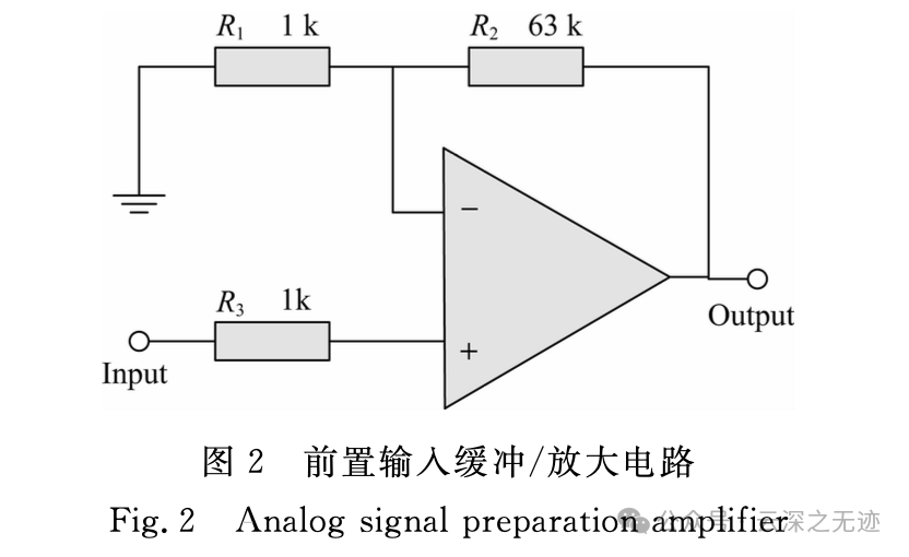
Channel A: Small Signal High Resolution (Microvolt Level)
Enhance the resolution of weak signals, suppress equivalent input noise in the 0.1–20 Hz band; use differential buffering/pre-amplification → ADS1255 (PGA=64, 50 SPS)
Preamplifier Selection:
Low voltage noise OP: e.g., LT1028 level (~0.85 nV/√Hz), but with higher current noise; suitable for low source impedance scenarios (the noise derivation example in the paper is based on such devices).
Chopper Zero Drift Type: e.g., ADA4522/ADA4528 series, very low 1/f noise, small temperature drift, better at low frequencies but requires handling chopper artifacts (easily seen in the 20–200 Hz band).
Channel A only covers the small signal range, with a short circuit noise of ~0.122 μV (50 SPS, value cited in the paper) for ADS1255 at PGA=64.
Channel B: Large Signal Wide Range (±40 V)
Avoid saturation from strong earthquakes and other large signals, maintain linearity and extend full scale; use precision resistor voltage divider network (level shifting/attenuation) → low noise buffering → ADS1255 (PGA=1)
Attenuation Ratio: Scale ±40 V (differential) down to the ADC acceptable range (the paper uses ±5 V; the implementation is equivalent to REF=5 V, PGA=1).
Target ratio: 8:1.
During design, differential symmetry is required, with the upper arm 392 kΩ×2, lower arm 49.9 kΩ×2 (0.1% or 0.01% thin film), each arm connected with a small capacitor (e.g., 2.2 nF) for first-order LP; after voltage division, a differential buffer (low offset, low noise, rail-to-rail input/output or sufficient headroom for power supply) is used. The bandwidth is similar to channel A, fc≈15–20 Hz, to avoid aliasing; considering the thermal noise of large resistors, appropriately reduce resistance values if necessary and balance input load.


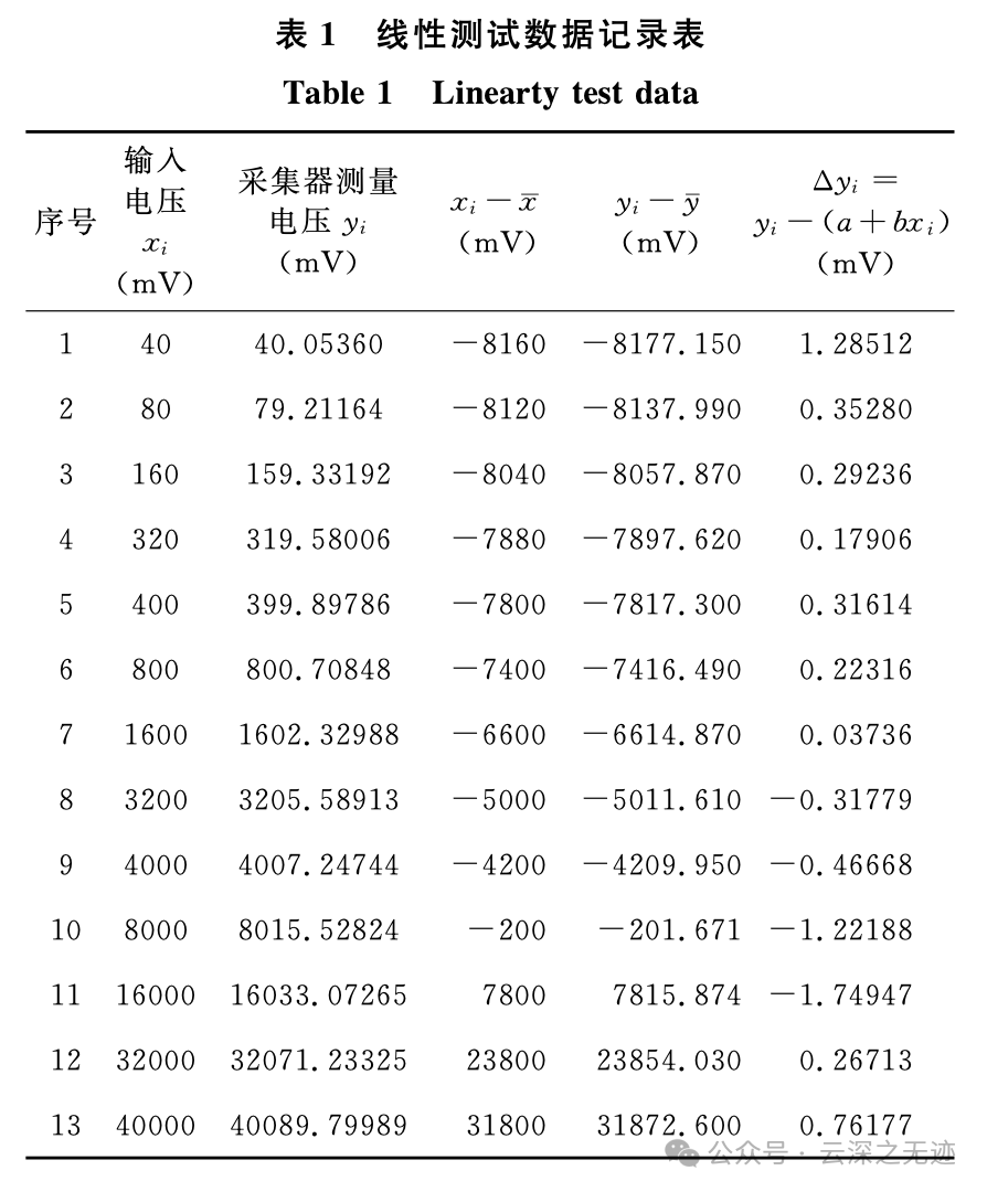
The input voltage <span>xi</span> ranges from 40 mV → 40000 mV (40 V), and the measured voltage <span>yi</span> remains consistent, indicating that the system uses voltage division + amplification before entering the ADC.
Minimum input point: 40 mV
Maximum input point: 40000 mV; the system must cover the voltage range of 0 ~ 40 V.
Voltage Division Conversion
Assuming the ADC full scale is ±2.5 V (common in high-precision ADCs):
High range channel: input 40 V → becomes 2.5 V after voltage division; the division ratio = 40 V / 2.5 V = 16; thus, a 1:16 voltage divider resistor network is needed (e.g., 160 kΩ : 10 kΩ).
Low range channel: if only measuring ±2.5 V, it can be directly input without voltage division.
Two ADCs’ Acquisition Ranges
Organized as follows:
| ADC Channel | Front-end Design | Input Range (Actual Voltage) | Corresponding ADC Input Range |
|---|---|---|---|
| Low Range ADC | Direct or small gain amplification | ±2.5 V | ±2.5 V |
| High Range ADC | 1:16 Voltage Divider Network | 0 ~ 40 V | 0 ~ 2.5 V |
Thus, the system can ensure high precision for small voltages while also accurately measuring large voltages.
Draw a “Dual-Range ADC Measurement Range Comparison Chart” (horizontal axis: actual input voltage 0~40 V, vertical axis: ADC mapped voltage 0~2.5 V, with two curves representing the coverage of the two channels)
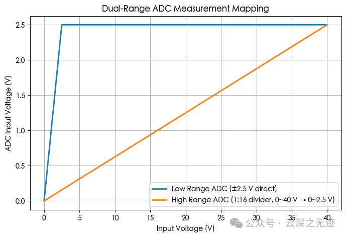
Small signals use low range ADC to ensure high resolution; large signals use high range ADC to ensure no distortion.
Blue Line (Low Range ADC)
Directly measures the input signal, with a linear range of only ±2.5 V; beyond this range, the output is compressed (saturated).
Orange Line (High Range ADC)
The input signal first goes through 1:16 voltage division, allowing it to cover 0~40 V, still mapping to the ADC’s ±2.5 V; the resolution is not high at low voltages.
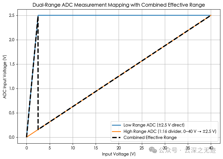
Black Dashed Line (Synthesis Curve)
For values less than ±2.5 V, the low range ADC is used (high resolution); for values greater than ±2.5 V, switch to the high range ADC (to prevent saturation); ultimately achieving a combination of 0~40 V input range + high resolution for small signals.
The interpretation is similar to the above.
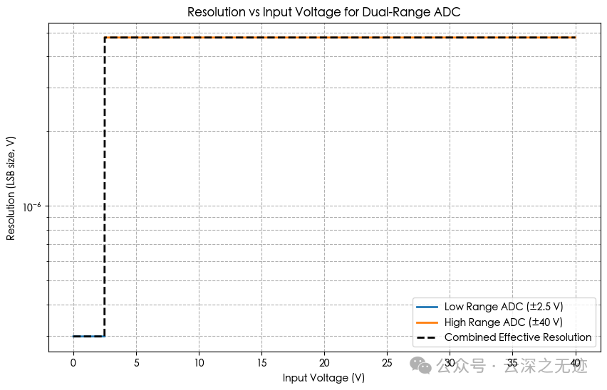
Calculate the Equivalent Dynamic Range of This Dual-Range Combination Scheme
Assuming limited by quantization noise only (24-bit, Vref = ±2.5 V)
The LSB of a single ADC: Quantization noise (RMS):
The maximum input (RMS) of the combined system:
Taking the minimum resolvable quantity from the small range channel (the best one):
Corresponding ENOB:
Note: Looking at any channel within its own range, the quantization limit DR is approximately 146.26 dB (independent of scaling). The dual-range expands the maximum measurable from ±2.5 V to ±40 V, while the minimum resolvable is still determined by the small range, thus the combined DR can exceed the single channel limit.
Based on Measured Noise (e.g., )
If using the common 157 dB from the paper, the system equivalent noise can be inferred to be approximately .
Theoretical Limit (Quantization Dominated): Approximately 170.3 dB / 28.0 bit.
Engineering Achievable (taking 0.2 µV_RMS as an example): Approximately 163.0 dB / 26.8 bit; the reported ~157 dB corresponds to a system combined noise of approximately 0.40 µV_RMS, consistent with actual factors such as power supply, reference, front-end noise, channel mismatch, and switching logic.
Anyway, since I haven’t seen the physical object, this is how it is calculated.

Teacher Tony sharply commented, just buy a 32-bit ADC, it’s not that expensive