
Improving the sampling accuracy of Analog-to-Digital Converters (ADC) is crucial for ensuring high-fidelity data conversion, involving various strategies and meticulous circuit design. What are the key measures? Let’s take a look~
1. Introduction to ADC and Performance Metrics
1.1 Brief Introduction to ADC
ADC stands for Analog-to-Digital Converter. Its function is to convert continuous analog signals into discrete digital signals for processing and analysis by digital systems. The type of ADC used in microcontrollers is the SAR (Successive Approximation Register) ADC, which is a successive approximation type of analog-to-digital conversion module.
ADC conversion includes four steps: sampling, holding, quantizing, and encoding.
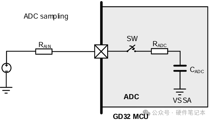
During the sampling phase, it is necessary to accurately sample the external signal voltage onto the ADC’s sampling capacitor within the specified sampling time. This occurs while the sampling switch SW is closed, allowing the external input signal to charge the sampling capacitor CADC through the external input resistance RAIN and the ADC sampling resistance RADC. Each sampling process can be simplified as the external signal charging the sampling capacitor through the input impedance and sampling resistance (i.e., the unit step response of the sampling capacitor at zero state). As follows:
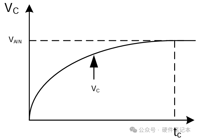
When the sampling time ends, the sampling error is represented as the voltage difference between the voltage on the sampling capacitor and the voltage at the signal source. In an ideal sampling process, this voltage difference should be maintained within 0.5 LSB (Least Significant Bit, which is the minimum voltage resolution of the SAR ADC; 0.5 LSB represents the quantization error of the SAR ADC).
During the quantization phase, the sampling switch SW is opened, and driven by the ADC clock, the voltage on the ADC sampling capacitor is compared sequentially with reference voltages of different weights using switched capacitor technology, determining the value of each bit of N-bit data (where N is the number of bits of the ADC) and then encoding the output digital code. During quantization, the reference voltage VREF+ needs to charge the switched capacitor network. The VREF+ reference must remain stable during quantization.
1.2 Performance Metrics of ADC
Resolution: Resolution indicates how many discrete levels the ADC can discretize the analog signal into, typically expressed in bits (e.g., 8-bit, 10-bit, 12-bit, etc.). The higher the resolution, the more accurately the ADC can quantify the analog signal.
Sampling Rate: The sampling rate refers to the number of times the ADC samples the analog signal per second. A higher sampling rate allows for a more accurate reconstruction of the original analog signal.
Signal-to-Noise Ratio (SNR): The SNR represents the ratio between the effective value of the signal and the effective value of the noise in the spectrum. Taking the logarithm and multiplying by 20 gives the SNR value in dB. This indicates the SNR between the digital signal output by the ADC and the input analog signal, i.e., the ratio of the effective signal to the noise. A higher SNR indicates better quality of the digital signal output by the ADC.
SNDR (Signal-to-Noise and Distortion Ratio): SNDR represents the effective power of the signal in the spectrum compared to the sum of the power of the noise and all harmonic components. Therefore, by definition, SNDR will always be less than SNR.
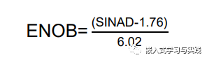
Effective Number of Bits (ENOB): In many applications, ENOB is used to describe the performance of the ADC. ENOB is typically calculated using the SNDR. Effective number of bits refers to the number of bits in the ADC output digital signal that contain valid information. It reflects the precision level of the ADC and is generally less than or equal to the resolution.
Device Accuracy: Device accuracy refers to the error between the digital signal output by the ADC and the input analog signal. It can be represented by the maximum non-linearity error, gain error, and offset error.
THD (Total Harmonic Distortion): Total harmonic distortion expresses the ratio of the effective value of the fundamental signal to the sum of the effective values of all harmonics.
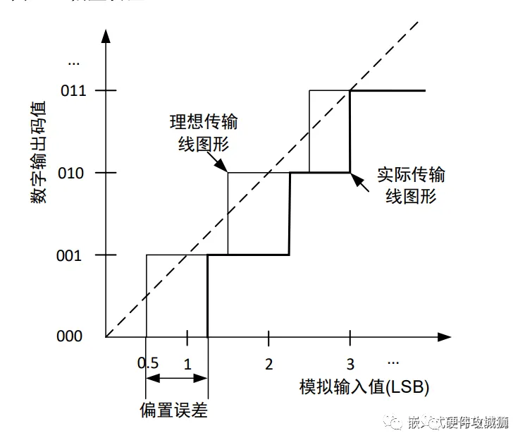
Offset Error: The offset error of the ADC is defined as the difference between the actual voltage corresponding to the first code transition (from 0x00 to 0x01) and the ideal voltage position.
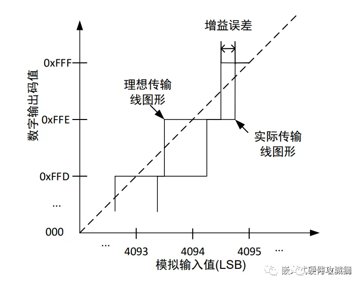
Gain Error: The gain error of the ADC refers to the difference between the actual conversion and the ideal conversion point voltage in the last code transition (for a 12-bit ADC, this is from 0xFFE to 0xFFF).
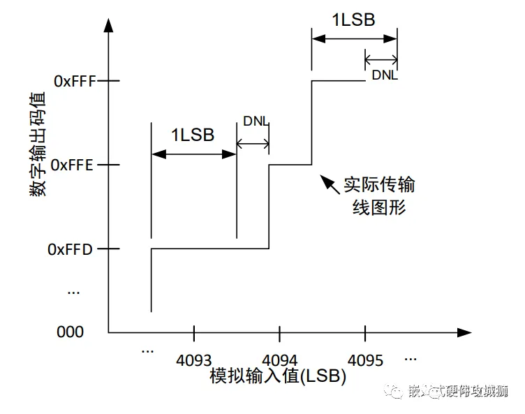
Differential Non-Linearity (DNL): Differential non-linearity is defined as the difference between the actual quantization step width and the ideal voltage value corresponding to 1 LSB. It indicates the degree to which each code width deviates from the ideal 1 LSB. The calculation method is the width of each code’s analog quantity minus the value of one LSB. When the code width is greater than one LSB width, DNL is positive; otherwise, DNL is negative.
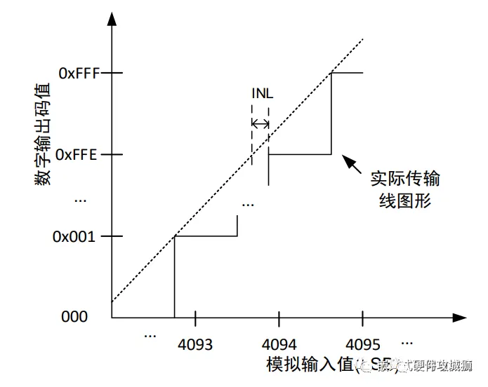
Integral Non-Linearity (INL): Integral non-linearity refers to the offset between the actual input point of a code and the ideal input on the transfer function line. The transfer function line can be defined as the line connecting the first actual conversion to the last actual conversion, i.e., a straight line between the ADC’s offset and gain error points.
In precision signal chain systems, the main focus for ADCs is often on the static characteristic parameters. However, for SAR ADCs with sampling rates reaching MSPS, they may also be used for sampling faster AC signals, making the true reproduction of AC input signals particularly important. In such scenarios, we pay more attention to the frequency domain characteristics of the signal. Some dynamic characteristic parameters also need to be considered, usually requiring FFT transformation of the sampled signal to analyze frequency domain characteristics.
These performance metrics may vary for ADCs in different application scenarios, and selecting the appropriate ADC requires weighing specific application needs.
The accuracy of the ADC is influenced not only by its design and process factors but also by various external factors. To achieve the nominal accuracy in practical applications, sufficient attention must be given to software configuration and the design of peripheral circuits.
2. Methods and Circuit Design to Improve ADC Sampling Accuracy
2.1 MCU Power Supply
In microcontrollers, some have the VREF+ pin brought out separately, while others do not, and the VREF+ pin is internally connected to VDDA. There is a precise internal reference source (typical voltage 2.5V) that can be used as the reference voltage for the ADC during operation. This internal reference voltage can be connected to the VREF pin, but it should be noted that this internal reference source has limited load capacity, so care should be taken in selecting the load size.
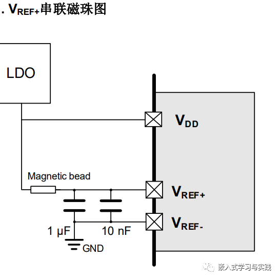
Since VREF+ needs to charge the conversion capacitor network during the quantization encoding process, and there will also be charge extraction from the reference source during quantization, if there are no other decoupling measures, a robust and clean VREF+ reference will significantly affect the ADC quantization accuracy. We recommend using LDOs with lower ripple noise coefficients to power these two sources. For the VREF+ reference source, we suggest placing a uF-level and a nF-level decoupling capacitor close to the pin, which can filter out low-frequency and high-frequency power noise from the outside and also stabilize the reference source during the ADC quantization encoding process. During layout, we recommend widening the power traces to reduce the ESR of the traces, minimizing the impact of the instantaneous charging of the conversion capacitor network on the input reference source during the quantization phase.
In similar situations, in some scenarios, if VDD and VREF+ come from the same LDO, a ferrite bead can be placed in series between the LDO and VREF+ to shield the external power supply’s influence on VREF+. When selecting the ferrite bead, attention should be paid to the RDC (DC resistance) parameter, and models with lower RDC should be prioritized to minimize the DC voltage drop across the ferrite bead. A lower DC resistance usually also results in lower impedance at high frequencies, making this a trade-off between anti-interference and sampling accuracy. Additionally, it is generally not recommended to replace the ferrite bead with an inductor in this case, as the VREF+ pin experiences high-frequency pulsed currents during quantization encoding. If the decoupling capacitors near the VREF+ pin are not set appropriately, it can easily cause voltage oscillations at VREF+, affecting the ADC’s accuracy.
2.2 Pin Capacitor Settings
Hardware decoupling in the system is particularly important for improving sampling accuracy. For the MCU, it is recommended to place a 1uF and a 10nF ceramic capacitor (with low ESR) close to the analog power pins. For other digital power VDD pins, a 100nF ceramic capacitor should be placed nearby. For the MCU ground pins, it is recommended to connect the analog ground and digital ground using a 0-ohm resistor or a ferrite bead to shield the digital ground’s interference on the analog ground.

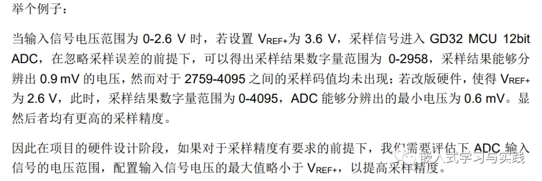
2.3 Impact of ADC Reference Voltage Settings
The input signal amplitude range for the ADC is from VSSA to VREF+. For some small package MCUs, VREF+ and VDDA are internally connected. The setting of the VREF+ voltage must strictly adhere to the specified range in the datasheet. The amplitude of the sampled signal should not exceed the amplitude of VREF+. For MCUs without a VREF+ pin, the amplitude of the sampled signal should not exceed the amplitude of VDDA; otherwise, it may lead to leakage in the analog power supply, severely affecting ADC performance. Additionally, we can consider how to set a reasonable VREF+ based on the ADC input signal amplitude range or how to set a reasonable ADC signal input range based on the configured VREF+.
2.4 Impact of Over-Range Voltage on I/O Pins
If there is a negative voltage (not exceeding -200 mV can be considered safe) on any analog pin (or adjacent digital input pin), it will introduce negative current flowing out from that I/O pin. This situation will significantly affect the ADC’s sampling results. To achieve more accurate sampling results, it is necessary to ensure that there is no negative voltage present on the relevant I/O pins during ADC operation.
During non-sampling times, the I/O pins for ADC sampling should not introduce voltages higher than VDDA, as this may cause leakage in the ADC core, leading to degraded sampling accuracy.
2.5 Impact of Signal Source Input Resistance
SAR ADC sampling has specific requirements for the input resistance of the signal. For a specific ADC, its sampling resistance RADC and sampling capacitance CADC are fixed. Once the sampling clock and sampling period are configured, the external signal’s input impedance has a maximum value requirement, as follows:
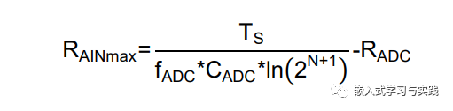
The maximum input resistance corresponding to different configured sampling periods will be provided in the datasheet for the corresponding MCU model, and users can also calculate it based on formulas and actual conditions.
The approach is as follows:
-
It is recommended to add a buffer amplifier circuit to achieve impedance matching;
-
If there are no sampling rate requirements, we can lower the ADC’s sampling clock, effectively increasing the sampling time to allow the sampling capacitor to charge to the correct potential.
For SAR ADCs, during the sampling time, the voltage on the sampling capacitor must be fully charged and discharged, and the voltage difference between the charged voltage and the external input voltage should not exceed 0.5 LSB; otherwise, regardless of how excellent the subsequent ADC performance is, it cannot accurately reflect the signal’s amplitude. For extremely high input impedance, we add a capacitor to limit the magnitude of voltage drops or spikes during a single sampling, but in this case, sufficient delay must be added between two samples to allow the internal sampling capacitor to charge, ensuring that the voltage difference between the sampling capacitor and the external signal remains within the quantization error range.
Particularly, when the ADC operates in continuous sampling or scanning sampling modes, if the input impedance is too high and not corrected in time, the sampling results of the channel with high input impedance will be influenced by the signal from the previous sampling channel. Increasing the sampling time to accommodate the input impedance effect will significantly improve this phenomenon.
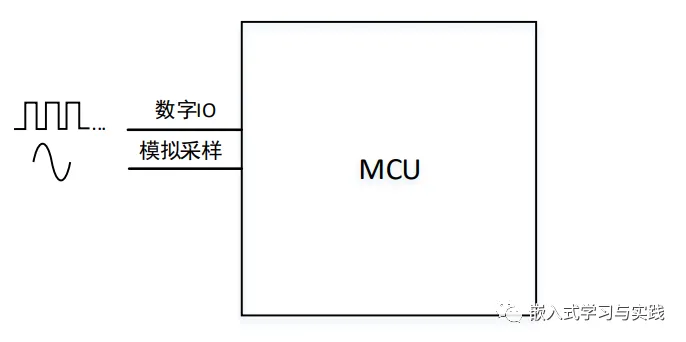
2.6 Impact of I/O Pin Crosstalk
Due to capacitive coupling between pins and even between bonding wires inside the chip, crosstalk between I/O can significantly affect the ADC’s sampling accuracy, especially when there are continuous digital I/O level transitions adjacent to the current ADC analog sampling channel (a typical case is PWM output).
The signal waveform of the ADC sampling channel adjacent to PWM output shows that during the level transition of PWM, there will be fluctuations in the signal on the adjacent sampling channel. If the ADC completes a sampling at this moment, it may result in significant errors in the sampling results.
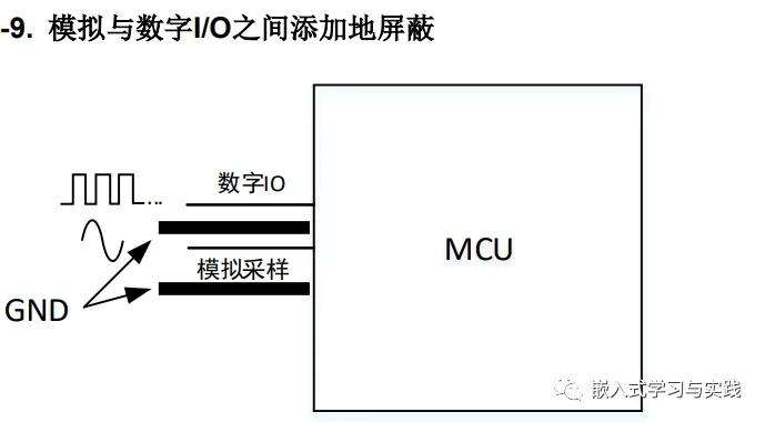
Several practical methods can be attempted to mitigate the impact of I/O crosstalk on ADC sampling. First, in pin planning, it is necessary to pre-plan to physically distance those digital I/O that need to flip continuously from the ADC sampling channel. If, due to resource constraints, frequently flipping digital I/O cannot be distanced from the analog sampling port, we can take some measures in the later layout to weaken the influence, such as adding a certain area of GND between the digital I/O and the analog channel for isolation.
Of course, since package grounding shielding cannot cover the internal chip, crosstalk between bonding wires will still exist. Additionally, slowing down the edges of digital signals can also reduce the impact of crosstalk, such as adding appropriately valued capacitors to digital signals to slow down the MCU digital I/O’s driving speed, which can significantly slow down the edges of these digital signals. On the software side, we also have some attempts, such as performing an ADC conversion when the digital I/O is not flipping, provided that the application allows it.
2.7 Software Methods to Improve ADC Sampling Accuracy
If the MCU has an on-chip hardware oversampling feature for the ADC, the hardware oversampling unit performs data preprocessing to reduce the CPU load. It can handle multiple conversions and average the results of multiple conversions to improve the accuracy of the ADC sampling results. This is achieved at the cost of reducing the data output rate in exchange for higher data resolution.
For MCUs without an on-chip hardware oversampling unit, common filtering algorithms can also be used in software to reduce fluctuations in the input signal sampling values. For example, the most common averaging algorithm requires CPU processing power and some RAM space during the filtering process. This averaging algorithm is suitable for situations where the input signal changes slowly, with occasional pulse-type interference. If the signal change frequency exceeds the execution frequency of this averaging filtering algorithm, the details of the signal change will be lost, and the averaged sampling results will not reproduce all the information of the signal.