Welcome to follow the public account belowAbao1990, this public account focuses on autonomous driving and smart cockpits, providing you with automotive insights every day. We start with cars, but we are not limited to them.

In the current context of intelligent driving sweeping the automotive industry, the term “camera” has become familiar to everyone. Many promotions even suggest that the more in-car cameras there are, the smarter the vehicle becomes. In fact, cameras have infiltrated almost every corner of our lives: smartphones, computers, community surveillance, smart doorbells… Nowadays, it is becoming increasingly difficult to find a scene without a camera.
However, despite our familiarity with cameras, if asked about their working principles, many people would still feel unfamiliar. How do cameras “see” the world? What signals do they output? What processing do these data undergo before being sent to AI models? This article will break down the working mechanisms behind cameras and show you how they see things.
Figure 1: A familiar yet unfamiliar schematic of a camera
Disassembling the tangible camera components
Let’s start by looking at the key components of in-car cameras from the most intuitive and tangible perspective.
Taking the ZF in-car camera shown in the figure as an example, its internal structure mainly consists of optical components and two core circuit boards (PCBs). The front end includes the lens and image sensor, which belong to the “optical sensing body”; the back end is the ISP module responsible for signal processing.
The role of the image sensor is to convert light signals into electrical signals, making it a core perception component. The example uses ON Semiconductor’s CMOS sensor.
The back-end signal processor is responsible for the “clear vision” task, processing and optimizing the raw images. The example uses a Mobileye chip, which not only has image signal processing capabilities but also integrates algorithms for target recognition and tracking.
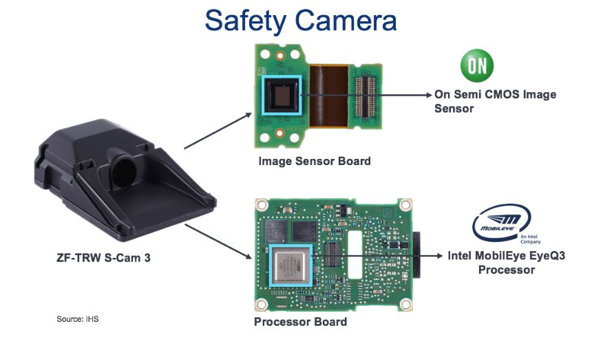
Figure 2: Schematic of an in-car camera
Above the image sensor is a set of precise optical structures, including protective layers, lenses, and lens mounts, ensuring that light is properly focused and filtered, ultimately landing accurately on the image sensor surface, laying the foundation for subsequent imaging.

Figure 3: Schematic of the relationship between the lens and image sensor
How does the image sensor “see”?
Next, let’s take a look at the microscopic structural principles of the image sensor, which are crucial for understanding how cameras can see things.
As shown on the left side of Figure 4, the image sensor is actually divided into many intersecting light-sensitive units, resembling a chessboard. Each tiny light-sensitive unit is what we commonly refer to as a “pixel”. For example, an image sensor with 3264 small units in width and 2448 small units in height has approximately 8 million pixels. The commonly referred 2 million pixels or 10 million pixels cameras correspond to the number of these smallest light-sensitive units. Naturally, the more pixels, the higher the image resolution.
As shown on the right side of Figure 4, when photons pass through the lens and enter the sensor, they first go through two layers of filters before reaching the semiconductor sensing layer that converts light signals into electrical signals.
Why are two layers of filters necessary?
Because photoelectric sensing essentially relies on the photoelectric effect of semiconductors, i.e., “light generates electricity”. However, in this effect, the strength of the electricity is mainly determined by the light intensity and is not sensitive to the wavelength of light (which corresponds to the colors we perceive). Therefore, the first layer needs to remove infrared and ultraviolet light that is not visible to the naked eye, leaving only the light we are interested in.
In visible light, we know that various colors can be synthesized using primary colors like red, blue, and green. However, a light-sensitive element within a pixel can only perceive one light intensity, meaning it has only one channel. So what should we do? Bryce Bayer, an engineer at Kodak and the inventor of the Bayer array, came up with a solution. He grouped four pixels in a square and deployed one blue, one red, and two green filters above the light-sensitive elements, allowing each pixel to capture the intensity of a single primary color. Based on this design, subsequent signal processing can approximate the restoration of the three primary color distributions at each pixel through interpolation. Why does green occupy half of the four squares? Because the human eye is most sensitive to green, hence this “bias”. And this colorful distribution, does it look familiar? That’s right, it’s a “mosaic”.
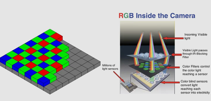
Figure 4: Schematic of the working principle of the image sensor
Within each pixel’s light-sensitive element, there are mainly two types: CCD and CMOS. Both utilize MOS technology, with CCD’s core component being a MOS capacitor, while CMOS’s core component is a MOSFET amplifier. The main difference is that CCD generates charges within each pixel and transmits them to the edge for unified amplification, while CMOS amplifies the current within each pixel.
To draw an analogy, CCD is like each employee reporting their work to a team leader after completing their tasks, and the team leader compiles a comprehensive report for the manager. This ensures that the content is refined and the format is consistent, resulting in high report quality, but the communication efficiency and production costs are higher. In contrast, CMOS is like each employee directly reporting their work to the boss after completing their tasks, which speeds up the reading process and reduces communication costs, but inevitably, the varying quality of employees may affect the report quality.
The comparison between CCD and CMOS is shown in the figure below. In scenarios such as in-car cameras and smartphone cameras, where power consumption, size, and cost are sensitive, CMOS image sensors have become the mainstream choice.
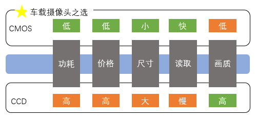
Figure 5: Comparison of differences between CCD and CMOS
Disassembling the architecture of ISP (Image Signal Processing)
After the photoelectric conversion and analog-to-digital conversion of the image sensor, the image sensor can now output the raw signals of the image by pixel, and by transmitting several frames of images per second, it can string them together to form an animation, creating a video. However, it should be noted that these raw images have many “flaws” and are far from what we see with the naked eye; they can be understood as “rough” images. They must undergo a series of image signal processing steps to be clearly visible. Next, let’s take a look at the common processing steps of ISP.
Step 1: Black Level Correction
This is essentially the “zeroing” of the sensor. Even when taking photos in the dark, the image sensor will output a non-zero voltage (black level). This step is to set “black as black”. It’s like taking a completely black photo, but the background color appears gray. We need to clean up the background first.
Step 2: Lens Shading Correction
The center of the lens is bright, while the edges are dark (due to optical characteristics). This step uses gain to make the image more uniform. It’s like shining a flashlight on the ground, where the center is bright and the surroundings are dark. We need to “fill in the light” around to make the image consistent.
Step 3: Bad Pixel Correction
It is not uncommon for some pixels on the image sensor to be defective: always bright, always dark, or with abnormal values, requiring repair. It’s like fixing “dust spots” on a photo by “erasing” them with surrounding colors.
Step 4: Demosaicing
As mentioned earlier, the Bayer Pattern uses an RGGB array filter to form a color mosaic, where each pixel only has one channel of color. We need to interpolate to complete the other two colors. It’s like a puzzle where only the red pieces are provided, and we need to deduce and piece together the complete color image.
Step 5: Auto White Balance
Under different light sources (such as yellow light, blue light), the color of the same object may deviate. White balance ensures that white appears consistently white. It’s like a white paper that appears yellow under a bulb and blue under sunlight. White balance corrects this “color cast”.
Step 6: Color Correction Matrix
The original colors from the image sensor may not match the true colors. A matrix mapping is used to correct color deviations. For example, the red captured by the image sensor may appear purple. The color correction matrix can pull it back to the true “bright red”.
Step 7: Local Tone Mapping
This enhances the local contrast of the image, making dark and bright details clearer, resulting in a more three-dimensional image. In simple terms, it brightens dark areas and lowers bright areas, enriching the details.
Step 8: Noise Reduction
Images, especially at night, can have a grainy appearance, requiring noise reduction while preserving details. It’s like reducing noise in a crackling recording without making the sound blurry.
Step 9: High Dynamic Range Merge
To avoid overexposure in bright areas and retain details in dark areas, multiple images with different exposures can be merged to achieve a higher dynamic range. In recent years, there have also been technologies that complete dynamic range synthesis from the image sensor side. For example, when a car rushes out of a tunnel: it needs to see both the dark areas inside the tunnel and the strong light at the exit. High dynamic range merging can help us achieve both.
Step 10: Gamma Correction
The human eye does not perceive brightness linearly, and gamma correction is intended to make the displayed image more aligned with human vision. This step involves nonlinear processing to make the image appear more “natural”.
Step 11: Sharpening
This enhances edge details and improves image clarity, making lane markings and traffic signs more prominent. It’s like applying edge enhancement to a blurry photo, making the contours clearer, suitable for perception models.
Step 12: Color Space Conversion
This converts RGB to encoding formats like YUV for video compression, display, or perception algorithms. RGB is “display-friendly”, while YUV is “compression-friendly”; for example, video encoding often uses the YUV420 format.
Of course, the steps of ISP in actual product applications vary and are adjusted based on sensor models and target applications (for example, for display on a vehicle’s large screen or for processing by AI models). Among these steps, the three that are particularly important for assisted driving are as follows, and we will further appreciate them through effect diagrams:
(1) High Dynamic Range Merge + Local Tone Mapping. Because there are many scenes with tunnels and backlighting, it is essential to see both dark pedestrians and bright lanes simultaneously.
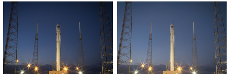
Figure 6: Schematic of high dynamic range and local tone mapping processing (left: before processing; right: after processing)
(2) Noise Reduction + Sharpening. This is crucial for the clarity of nighttime images, directly affecting the performance of lane line recognition and object detection.
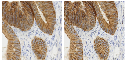
Figure 7: Schematic of noise reduction and sharpening (left: before processing; right: after processing)
(3) White Balance + Color Correction Matrix. Since assisted driving generally uses multiple cameras simultaneously, this processing ensures the consistency of multi-camera calibration; otherwise, it would affect stereo matching and perception model training.

Figure 8: Schematic of white balance and color correction (left: before processing; right: after processing)
Transmission between the front-end module and ISP
Having discussed the image sensor and ISP, we understand the two parts of “seeing” and “seeing clearly”. Now the question arises: how are these two parts connected?
The most direct method is to connect them with a high-speed line. The most commonly used transmission method is MIPI CSI-2 (Camera Serial Interface 2), a high-speed serial interface defined by the MIPI Alliance. For intelligent camera systems, the front-end camera module and ISP processing chip are integrated within a single system controller.
However, with the development of assisted driving technology, more and more solutions have adopted multiple edge camera modules arranged at different positions on the vehicle, and then the data from the image sensors are transmitted to a central controller located, for example, under the trunk for processing. In this case, the transmission distance between the front-end sensor module and the back-end ISP can reach several meters, and directly using MIPI CSI-2 cables for transmission can lead to severe signal attenuation, making reliable transmission impossible. Therefore, we introduce SerDes (Serializer/Deserializer) for the following processing:
(1) Serializer: Converts the MIPI parallel or low-speed serial data from the camera module into high-speed serial signals (such as GMSL, FPD-Link).
(2) High-speed transmission: Uses automotive-specific long-distance high-speed cables (such as coaxial cables or shielded twisted pairs) for long-distance transmission.
(3) Deserializer: At the ISP end (i.e., within the domain controller), it restores the high-speed serial signals back to MIPI CSI-2 format for ISP processing.
In summary, if the camera is close to the processor (within the same controller), MIPI can be used directly; if the camera is far from the processor (not within the same controller), serial-deserialization technology is needed for transmission.
Current Industry Trends
As the level of intelligence in vehicles continues to rise, in-car cameras, as one of the core sensors for environmental perception, are seeing an increase in both installation volume and technical requirements. According to predictions from organizations like Strategy Analytics, global shipments of in-car cameras will exceed 600 million by 2025, with the Chinese market accounting for over 40%, becoming the largest single market in the world.
Driven by scenarios such as L2++, DMS, and APA, the average number of cameras installed in new cars in China is moving from 6 to over 10. Not only is the number of cameras increasing, but their types are evolving from a single rearview camera to multiple deployments throughout the vehicle, widely covering core aspects of perception, safety, and interaction. In the past, core industry technologies were long dominated by Japanese and American companies, but in recent years, domestic Chinese manufacturers have achieved rapid breakthroughs at multiple nodes and have gradually established a complete independent supply chain system.
In the optical lens segment, Sunny Optical is globally leading, with complete automotive-grade mass production and system capabilities. Other manufacturers like United Optics and Fucjeng Technology are also accelerating their layouts to promote the increase of domestic penetration rates.
In the field of CMOS image sensors, OmniVision leads the way, with its products achieving mass production in front-view, surround-view, and DMS scenarios, holding a market share among the top three globally. New forces like GalaxyCore and SmartSens are positioning themselves in the mid-to-low-end segmented markets.
The ISP chip segment is still dominated by Horizon Robotics, Black Sesame, NVIDIA, Qualcomm, and Ambarella, with domestic companies still in the catch-up phase, but many products have already been mass-produced and deployed in vehicles.
For us automotive practitioners, this is undoubtedly a positive development. At the same time, we must seize opportunities, especially by gaining more exposure and understanding of upstream and downstream technologies, enhancing our competitiveness through “cross-border” approaches. For example, those involved in image processing should not only excel in tuning but also “understand algorithms”, learning more about front-end AI processing and visual enhancement algorithms, which will give them more voice when communicating with perception engineers. Salespeople can also start from the technical pain points of customers, discussing scenarios and technologies to become solution-oriented salespeople. The Chinese in-car camera industry is undergoing a critical phase of transformation from “quantitative change” to “qualitative change”. Whether you are a research and development engineer, product manager, or a practitioner interested in assisted driving, do not miss this golden window for the rise of domestic products.
Image source: Internet, please contact for removal if there is any infringement.
A group of like-minded friends gather in the Knowledge Circle
Join the “Abao Talks Cars” Knowledge Circle to obtain relevant learning materials for these modules (currently including research reports, online expert sharing, and offline closed-door meetings), covering 16 major sections, with a detailed list as follows:
