In the current global wave of intelligent driving, cameras have become one of the essential core sensors in automotive perception systems. They not only give vehicles the ability to “see” but also provide foundational data support for subsequent AI model recognition and decision-making. Although we use the cameras on our phones or computers every day, our understanding of their working mechanisms may not be deep. This article will systematically break down the entire process of how cameras “see,” from hardware construction to image processing, and industry trends, revealing the “visual code” of cameras from all angles.
1. Evolution of Camera Development
1. Analog Camera Era (1980s-2000s)Early cameras primarily transmitted analog signals, using CCD sensors, with resolutions generally below 1 million pixels. Typical applications included security monitoring and industrial inspection, but limited by transmission distance and image quality, their functions were singular. In 1991, the University of Cambridge in the UK launched the world’s first network camera, “CoffeeCam,” marking the dawn of digital cameras.
2. Digital Network Camera Era (2000s-2010s)With breakthroughs in CMOS sensor technology, cameras entered the era of millions of pixels. In 2006, infrared night vision technology became widespread, and digital network cameras gradually replaced analog devices, supporting remote access and storage. The rise of smartphones propelled the implementation of multi-camera solutions, such as the Nokia 808 PureView in 2011, which featured a 41-megapixel single camera, achieving the breakthrough of “smartphones replacing cameras” for the first time.
3. Intelligent Camera Era (2010s – Present)
Multi-camera and high pixel: Huawei Mate40 Pro features a rear five-camera combination (50MP ultra-sensing + 20MP ultra-wide + 12MP telephoto + laser focus + 3D depth sensing), covering all scene shooting needs.
3D sensing technology: The iPhone X first introduced structured light solutions (TrueDepth camera), enabling Face ID and AR interactions; by 2025, ToF (Time of Flight) technology became mainstream, with the Sony IMX681 chip monopolizing the smart glasses market.
Upgrades in automotive cameras: The Tesla Model Y 2025 version is equipped with 11 cameras (including stereo vision), using the HW4.0 hardware platform to achieve 360-degree ultra-high-definition perception. BMW iX has added an interior camera to support anti-theft monitoring and passenger status recognition.
AI integration: Edge computing architectures (such as 5TOPS computing power chips) enable cameras to have real-time intelligent analysis capabilities, reducing the false alarm rate from 15% to 0.3%.
2. Disassembly of Cameras;Hardware Architecture
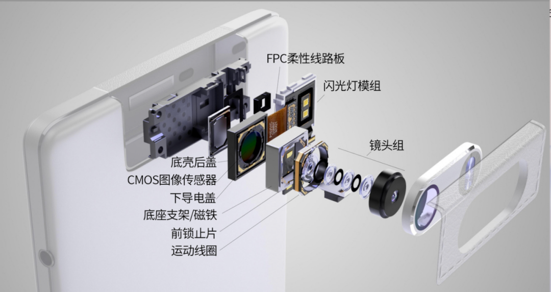
Optical System: The lens group (glass/ plastic mixed lens) is responsible for focusing light, while the aperture controls the amount of light entering. Periscope lenses achieve optical zoom of more than 5 times by folding the light path, such as in the Huawei P30 Pro.
Image Sensor:
1. CCD vs CMOS: CCD has high sensitivity but high power consumption, while CMOS is low-cost and highly integrated, becoming mainstream. Sony’s IMX series sensors use back-illuminated (BSI) technology, improving quantum efficiency by 30%.
2. Global Shutter vs Rolling Shutter: Global shutter exposes all pixels simultaneously, suitable for high-speed motion scenes (such as ADAS); rolling shutter exposes line by line, which may cause jelly effects but is cheaper.
Signal Processing: The ISP (Image Signal Processor) executes algorithms for noise reduction, HDR composition, auto-focus, etc. The Mobileye EyeQ5H chip supports 11 camera inputs, with processing delays under 100ms.
Taking automotive cameras as an example, their internal structure mainly consists of optical components and two core circuit boards ( PCB) that make up the system. The front end consists of the lens and image sensor, which belong to the “optical sensing body”; the back end is responsible for signal processing via the ISP module.
Among them, the role of the image sensor is to convert light signals into electrical signals, which is a core perception component.
Meanwhile, the signal processor at the back end is responsible for the task of “seeing clearly,” processing and optimizing the raw images. The example used is the Mobileye chip, which not only has image signal processing capabilities but also integrates algorithms for target recognition and tracking.
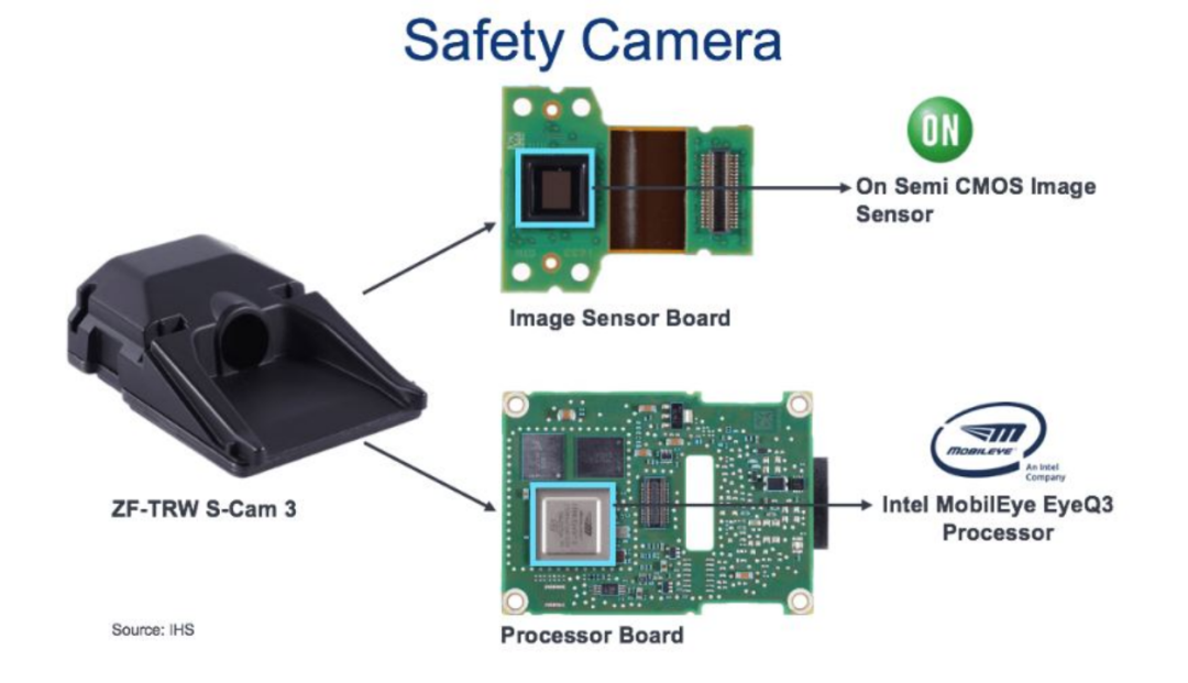
Above the image sensor is a set of precision optical structures, including protective covers, lenses, and lens mounts, ensuring that light is focused and filtered as necessary, ultimately landing accurately on the surface of the image sensor, laying the foundation for subsequent imaging.
3. How Does the Image Sensor “See”?
Image sensors are the physical basis for cameras to achieve “visual perception”; their core function is to convert light signals into electrical signals through the photoelectric effect and to discretely sample spatial information through a pixel array.
Image sensors are like a chessboard, divided into many intersecting light-sensitive units. Each tiny light-sensitive unit is what we commonly refer to as a “pixel.” For example, an image sensor with a width of 3264 small units and a height of 2448 small units has approximately 8 million pixels. The commonly referred 2 million pixel or 10 million pixel cameras correspond to the number of the smallest light-sensitive units. Naturally, the more pixels, the higher the image resolution.
When photons pass through the lens and enter the sensor, they first go through two layers of filter layers before reaching the semiconductor sensing layer that converts light signals into electrical signals.
The Dual Mission of the Filter Layers
First Layer: Infrared Cut Filter (IR Cut Filter)
Silicon-based multilayer coatings (such as TiO₂/SiO₂ alternating deposition) reflect infrared light (wavelength > 760nm) and ultraviolet light (<400nm) through interference effects, allowing only visible light (400-760nm) to pass through.
Function: To prevent infrared light from interfering with human visual perception (for example, infrared radiation from car lights at night may cause the image to appear washed out). Since the photoelectric sensing essentially relies on the photoelectric effect of semiconductors, which is “light generates electricity.” However, the strength of the electricity in this effect is mainly determined by the light intensity and is not sensitive to the wavelength of light (corresponding to the colors we perceive), so the first layer needs to remove infrared and ultraviolet light that are not perceived by the naked eye, leaving only the visible light that can be recognized.
Within visible light, we know that various colors can be synthesized through primary colors like red, blue, and green. However, a light-sensitive element within a pixel can only perceive one light intensity, meaning it has only one channel, thus Bryce Bayer, an engineer at Kodak, who is also the inventor of the Bayer array, came up with a solution (Bayer pattern).
Second Layer: Bayer Color Filter Array (CFA)
Array Structure: 4 pixels form a group (2×2 matrix), arranged in an “RGGB” pattern (1 red, 1 blue, 2 green), as described in the document “the human eye is sensitive to green, hence green accounts for 50%”.
Interpolation Algorithm (Demosaicing): Each pixel captures only a single color channel and needs to interpolate neighboring pixels to restore the full-color image. Typical algorithms include:
Bilinear Interpolation: Estimates the missing channel based on the average of adjacent pixels, simple to compute but may blur edges.
Adaptive Interpolation: Selects interpolation weights based on the gradient direction of the image to reduce color artifacts (such as purple edges on mosaic edges).
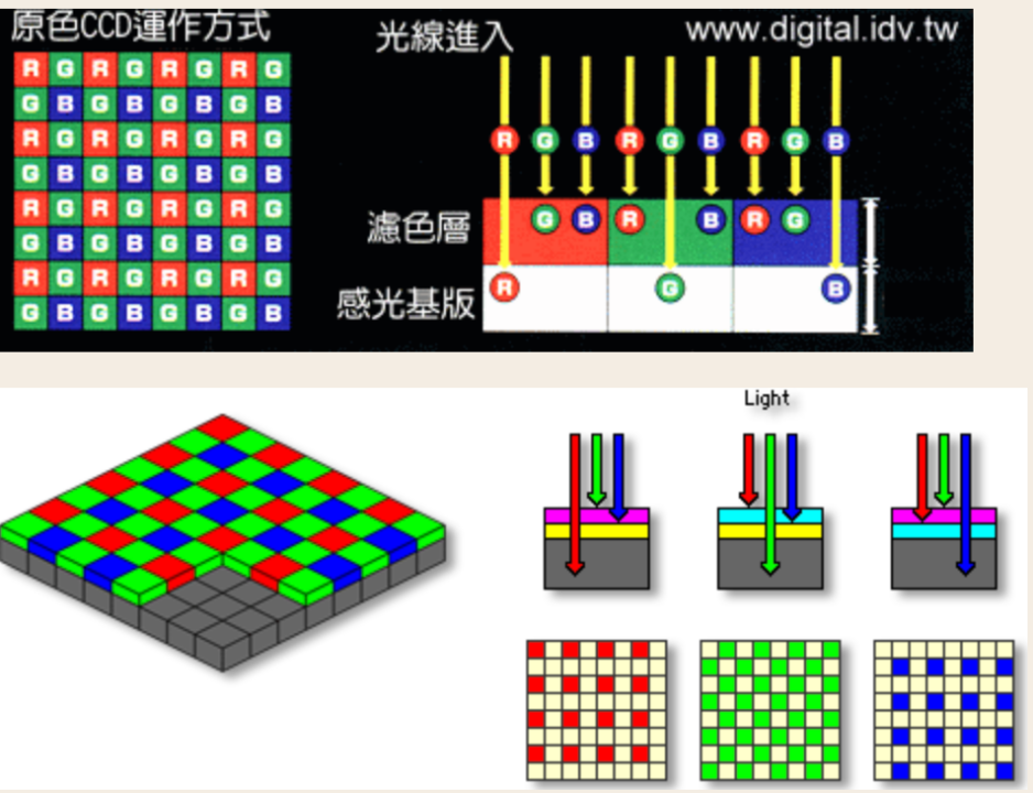
In each pixel’s light-sensitive element, there are mainly two types: CCD and CMOS. Both use MOS technology; the core component of CCD is the MOS capacitor, while the core component of CMOS is the MOSFET amplifier. The main difference is that CCD generates charges within each pixel and transfers them to the edge for unified amplification, while CMOS amplifies current within each pixel.
3. Technical Differences Between CMOS and CCD
| Characteristics | CMOS Sensor | CCD Sensor |
|---|---|---|
| Core Component | MOSFET amplifier (independent amplification for each pixel) | MOS capacitor (global charge transfer followed by centralized amplification) |
| Signal Path | Charge-voltage conversion is completed within the pixel, directly outputting electrical signals | Charge is transferred line by line through a shift register to the edge amplifier |
| Power Consumption | Low (single pixel power consumption about 100nW) | High (charge transfer requires clock driving, power consumption is 1-2 orders of magnitude higher) |
| Reading Speed | Fast (supports rolling shutter or global shutter) | Slow (line-by-line transfer limits frame rate) |
| Noise Characteristics | Exists line noise and fixed pattern noise (requires ISP correction) | High noise consistency, suitable for low-light environments (such as astronomical observation) |
| Cost | Low (high integration, single chip completes sensing + amplification) | High (requires independent driving circuits, complex manufacturing process) |
Logic for selecting automotive scenarios: Automotive cameras need to balance power consumption (limited by vehicle batteries), cost (for mass production), and vibration resistance ( CMOS chips have high integration and stronger mechanical stability), thus over 95% of models use CMOS solutions (such as ON Semiconductor AR0234 sensors)
ISP Image Signal Processing: From “Raw” to “Finished Product” Production Line
The raw output from the image sensor is RAW format data (such as RGGB mosaic image + dark current noise), which needs to undergo 12 processing steps by the ISP chip (as detailed in the third part of the document). Below are the technical details of key steps:
Step 1: Black Level Correction
This essentially is the sensor’s “zeroing.” Even in darkness, the image sensor outputs a non-zero voltage (black level). This step is to set “black to black.” It’s like taking a picture in complete darkness, but the background color appears gray. We need to clean up the background first.
Step 2: Lens Shading Correction
The center of the lens is bright, while the edges are dark (due to optical characteristics). This step uses gain to make the image more uniform. It’s like shining a flashlight on the ground, where the center is bright and the surroundings are dark. We need to “fill in the light” around to make the image consistent.
Step 3: Bad Pixel Correction
It is possible that some pixels on the image sensor are defective: always bright, always dark, or with abnormal values, which need to be repaired. It’s like fixing “dust spots” on a photo by “erasing” them with surrounding colors.
Step 4: Demosaicing
As mentioned earlier, the Bayer Pattern forms a color mosaic with the RGGB array filter, where each pixel only has one color channel, and we need to interpolate to complete the other two colors. It’s like a puzzle that only provides red pieces, and we need to infer and piece together the complete color image.
Step 5: Auto White Balance
Under different light sources (such as yellow light, blue light), the color of the same object may deviate. White balance ensures that white appears consistently white. It’s like a white paper that appears yellow under a bulb and blue under sunlight. White balance corrects this “color cast.”
Step 6: Color Correction Matrix
The original colors from the image sensor may not match the true colors. A matrix mapping is used to correct color deviations. For example, the red captured by the image sensor may appear purple. The color correction matrix can pull it back to the true “red color.”
Step 7: Local Tone Mapping
Enhances local contrast in the image, making dark/light details clearer, resulting in a more three-dimensional image. In simple terms, it brightens dark areas and compresses bright areas, enriching details.
Step 8: Noise Reduction
Images, especially at night, can have graininess, requiring noise reduction while preserving details. It’s like reducing noise in a crackling recording without making the sound blurry.
Step 9: High Dynamic Range Merge
To avoid overexposure in bright areas while retaining details in dark areas, multiple images with different exposures can be merged to achieve a higher dynamic range. In recent years, there have been technologies that complete dynamic range synthesis at the image sensor end. For example, when a car emerges from a tunnel: it needs to see both the dark areas inside the tunnel and the strong light at the exit. High dynamic range synthesis can help us achieve both.
Step 10: Gamma Correction
The human eye does not perceive brightness linearly; gamma correction is used to make the displayed image more in line with human vision. This step performs non-linear processing to make the image look more “natural.”
Step 11: Sharpening
Enhances edge details, improving image clarity, making lane markings and traffic signs more prominent. It’s like applying edge enhancement to a blurry photo, making the contours clearer, suitable for perception models.
Step 12: Color Space Conversion
Converts RGB to encoding formats like YUV for video compression, display, or perception algorithms. RGB is “display-friendly,” while YUV is “compression-friendly,” with YUV420 format commonly used in video encoding.
4. Transmission Between Front-End Modules and ISP
In the automotive camera system, the image transmission process between the front-end module and the back-end ISP (Image Signal Processor) is crucial. It determines whether image data can be delivered to the processing platform with high quality, low latency, and high reliability, especially in multi-camera and distributed deployment of intelligent vehicle architectures. Below is a detailed analysis of this transmission process:
1. Basic Relationship Between Front-End Module and ISP
Camera Front-End Module
Includes: lens group, filters, image sensors (such as CMOS), and basic driving circuits.
Function: To collect environmental light and convert it into electrical signals (image data).
ISP (Image Signal Processor)
Location: Inside the vehicle domain controller (such as ADAS domain control).
Function: To process raw image data, such as noise reduction, white balance, HDR composition, etc., to make it “see clearly.”
2. Common Connection Methods
Short-Distance Connection: MIPI CSI-2 Interface
When the camera module and ISP are in the same PCB or the same controller module (such as in-vehicle central control cameras), MIPI CSI-2 (Camera Serial Interface-2) is commonly used:
Characteristics: High-speed serial transmission, rates up to 6Gbps+, simple structure, low power consumption, using differential pairs (usually 2-4 pairs of signal lines) for point-to-point communication.
Application Scenarios: In-vehicle DMS, CMS, or rearview cameras, etc., with short wiring layouts.
Long-Distance Connection: SerDes (Serializer/Deserializer) System
In multi-camera systems, modules are often deployed around the vehicle (such as front/rear/side view, surround view systems), with transmission distances of several meters. Directly transmitting signals via MIPI would result in significant attenuation, hence the introduction of SerDes technology:
Transmission Process:
| Step | Module | Function |
|---|---|---|
| 1 | Serializer | Converts the parallel data output from the front-end image sensor (MIPI / LVDS) into high-speed serial signals (such as GMSL, FPD-Link). |
| 2 | High-Speed Transmission Cable | Uses automotive-grade long-distance cables (such as shielded twisted pairs, coaxial cables) for transmission. |
| 3 | Deserializer | Restores high-speed serial signals to a standard format recognizable by the ISP (such as MIPI CSI-2), passing it to the back-end ISP for processing. |
3. Advantages of the SerDes System
| Advantages | Description |
|---|---|
| Long-Distance Transmission | Can achieve distortion-free transmission over distances exceeding 10 meters, suitable for vehicle wiring. |
| High Bandwidth | Supports transmission rates up to 12Gbps+, meeting the output requirements of high-definition cameras. |
| Integrated Power Supply Channel | Coaxial cables support Power over Coax (PoC), simplifying wiring. |
| EMI Interference Resistance | Shielded cable structures have excellent electromagnetic compatibility. |
| Multiplexing | A single cable can reuse synchronization signals, control commands, etc., simplifying system design. |
5. Industry Trends in Automotive Cameras
1. High Resolution and Pixel Upgrades Automotive cameras are transitioning from 2 million – 8 million pixels to 12 million – 20 million pixels, with 8MP (29MPixel) front-facing cameras becoming standard for L2+ models (such as Tesla HW4.0), capable of recognizing traffic signs 200 meters away. Sensors like Sony IMX675 support 4K resolution, with HDR technology enhancing dynamic range to 140dB, meeting the needs of complex scenarios like tunnels and strong light.
2. Multi-Camera Fusion and Comprehensive Perception The number of cameras per vehicle has increased from 3-5 to 8-12, covering front, surround, interior, and side views. For example, the NIO ET9 is equipped with 11 cameras, including 4 laser radar-level 8MP lenses, achieving 360° coverage without blind spots. Multi-camera fusion solutions (such as stereo vision + surround view) improve distance measurement accuracy to 0.1 meters, with nighttime obstacle detection rates increasing from 75% to 92%.
3. Intelligence and Edge Computing Integration ISP chips integrate AI acceleration units (such as Horizon Journey 6 supporting 16TOPS computing power), enabling lane line recognition, pedestrian detection, and other preprocessing on the edge, reducing latency from 100ms to 30ms. The Mobileye EyeQ6 chip supports 14 camera inputs, with a built-in neural network accelerator that directly outputs target bounding box coordinates, reducing reliance on the computing power of domain controllers.
4. Solid-State Lenses and New Material Applications Traditional voice coil motor (VCM) focusing solutions are gradually being replaced by solid-state lenses, using MEMS micro-electromechanical technology (such as STMicroelectronics solutions), improving focusing speed from 200ms to 20ms and enhancing vibration resistance by 5 times (suitable for automotive bumpy environments). In terms of optical materials, hybrid lenses (glass + plastic) have reduced costs by 20%, and Sunny Optical’s 8P glass lens yield has exceeded 90%.
5. Proliferation of Electronic Rearview Mirrors and Regulatory Drivers The GB 15084-2022 standard implemented in China in July 2023 allows electronic rearview mirrors to replace traditional glass mirrors, with Toyota, BYD, and others being the first to pilot. Electronic rearview mirror cameras have a resolution of 2MP, using algorithms to eliminate glare from rain and night, expanding the field of view by 30%, with an expected penetration rate exceeding 30% by 2025.
Source: Official and online comprehensive descriptionsProduced by: Smart Driving π