In the pursuit of extreme performance in computers and servers, overclocking has become the “holy grail” for hardware enthusiasts and high-performance computing scenarios. By breaking through the frequency limits set by manufacturers, core chips such as CPUs and GPUs can unleash computational power far beyond their rated specifications. Behind this, high-frequency high-speed printed circuit boards (PCBs) have emerged, serving not only as the physical carrier for chips but also as the critical “highway” and “heat dissipation base” that ensure successful overclocking. This article will explore how PCBs can meet the stringent demands of overclocking through advanced materials science, precision manufacturing processes, and collaboration with hardware and software.
1. Overclocking: Performance Leap and Challenges
1. What is Overclocking?
Overclocking refers to the technique of manually adjusting hardware parameters (such as core voltage, multiplier, front-side bus frequency, etc.) to make them operate at frequencies exceeding the safe values set by manufacturers. The principle behind this is that chip manufacturers typically set conservative frequency limits to ensure a high yield and stability in mass production. However, many high-quality chips have the potential to run at higher frequencies under enhanced cooling and appropriate voltage increases. Overclocking can significantly enhance the performance of core components such as CPUs, GPUs, and memory, especially in scenarios like gaming, scientific computing, and data centers, leading to direct benefits such as increased frame rates and reduced computation times.
2. Hardware Foundations and Challenges of Overclocking
Overclocking primarily affects two core hardware components:
Chip (CPU/GPU): This is the direct target of overclocking. Increasing frequency requires raising core voltage to maintain signal stability, but this leads to a dramatic increase in power consumption and heat generation (power consumption is proportional to the square of frequency and voltage). Therefore, the “quality” of the chip (the variability of the manufacturing process) and the cooling solutions are fundamental to successful overclocking.
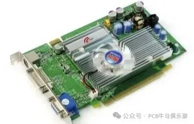
PCB (Printed Circuit Board): As the platform that carries chips, power modules, memory chips, and other critical components, the PCB plays a “behind-the-scenes hero” role in overclocking. The challenges it faces mainly come from two aspects:
* Signal Integrity Challenges: The higher the frequency, the shorter the signal wavelength, making it extremely sensitive to any imperfections in the transmission path (such as impedance discontinuities, crosstalk, reflections), which can easily lead to data errors and system crashes.
* Power Supply and Heat Dissipation Challenges: During overclocking, chip power consumption may increase by 50% or more, requiring the PCB to provide an extremely stable and clean power supply (low ripple, low noise), while also effectively conducting and dissipating the significant heat generated by the chips and power modules.
2. High-Frequency High-Speed PCB Materials: The Cornerstone of Signal Highways
To address the signal integrity challenges posed by overclocking, the choice of PCB materials is crucial. Traditional FR-4 materials suffer from excessive loss at high frequencies and can no longer meet the demands. High-frequency high-speed materials are preferred for overclocking PCBs due to their low dielectric constant (Dk) and low loss factor (Df).
Low Dk/Dk Stability: The dielectric constant (Dk) affects the transmission speed of signals in the PCB. A low and stable Dk value ensures consistent signal transmission delays, reducing timing errors, which is critical for precise signal synchronization at high frequencies (such as memory overclocking).
Low Df (Loss Factor): This is a key indicator of the energy loss of signals during transmission. The lower the Df, the smaller the signal attenuation, the longer the transmission distance, and the greater the eye diagram opening, leading to higher system stability. At frequencies above 10GHz, the Df of ordinary FR-4 is about 0.02, while high-frequency materials such as PTFE (polytetrafluoroethylene) can have a Df as low as 0.0013, Rogers RO4350B has a Df of 0.0037, and Panasonic Megtron series can have a Df as low as 0.0017. This order of magnitude reduction fundamentally ensures the integrity of signals under overclocking conditions.
Mainstream High-Frequency High-Speed Material Systems Include:
* PTFE (Polytetrafluoroethylene) Substrates (such as Rogers RO3003, Taconic TLY-5): These have ultra-low Df (≤0.002) and excellent frequency stability, making them the first choice for millimeter-wave (≥30GHz) applications. However, they are difficult to process (requiring high-temperature lamination), expensive, and have poor adhesion to traditional FR-4.
* Hydrocarbon Resin (PCH)/Ceramic-Filled Modified Materials (such as Rogers RO4000 series, Shengyi S1000-2G): By adding ceramic fillers to hydrocarbon resins to optimize performance, they achieve Df < 0.0028, balancing good performance, cost, and processability, widely used in servers and high-end graphics cards.
* Polyphenylene Ether (PPO) Substrates (such as Panasonic Megtron6/7): Df can be as low as 0.002 (Megtron6) or 0.0017 (Megtron7N), with excellent CAF (Conductive Anodic Filament) resistance, particularly suitable for high-density interconnect (HDI) boards and data center server motherboards, high-speed optical modules, etc.
Key Process Coordination in PCB Manufacturing:
* Hybrid Lamination Technology: To balance cost and performance, PCB manufacturers often splice high-frequency materials with ordinary FR-4 as needed. For example, using PTFE or modified epoxy materials in high-speed signal areas around the GPU core and video memory, while using FR-4 in other low-speed areas. This requires addressing the thermal expansion coefficient (CTE) matching and bonding issues between different materials, often using surface treatment technologies like plasma etching to enhance interface bonding strength.
Low Roughness Copper Foil (VLP): High-frequency signals exhibit the “skin effect,” where current concentrates on the surface of the copper foil. Using rolled copper (Ra ≤ 0.3μm) instead of ordinary electrolytic copper (Ra ≈ 1.5μm) can significantly reduce conductor losses, further decreasing signal attenuation.
Precision Impedance Control: Signals under overclocking are extremely sensitive to impedance deviations (within ±5%). PCB manufacturers precisely control the dielectric thickness using laser thickness gauges, combined with etching compensation techniques (line width error ±0.01mm), and use network analyzers for full inspection to ensure the accuracy and consistency of differential line impedance (such as PCIe 5.0 requirements of 85Ω ±5%).
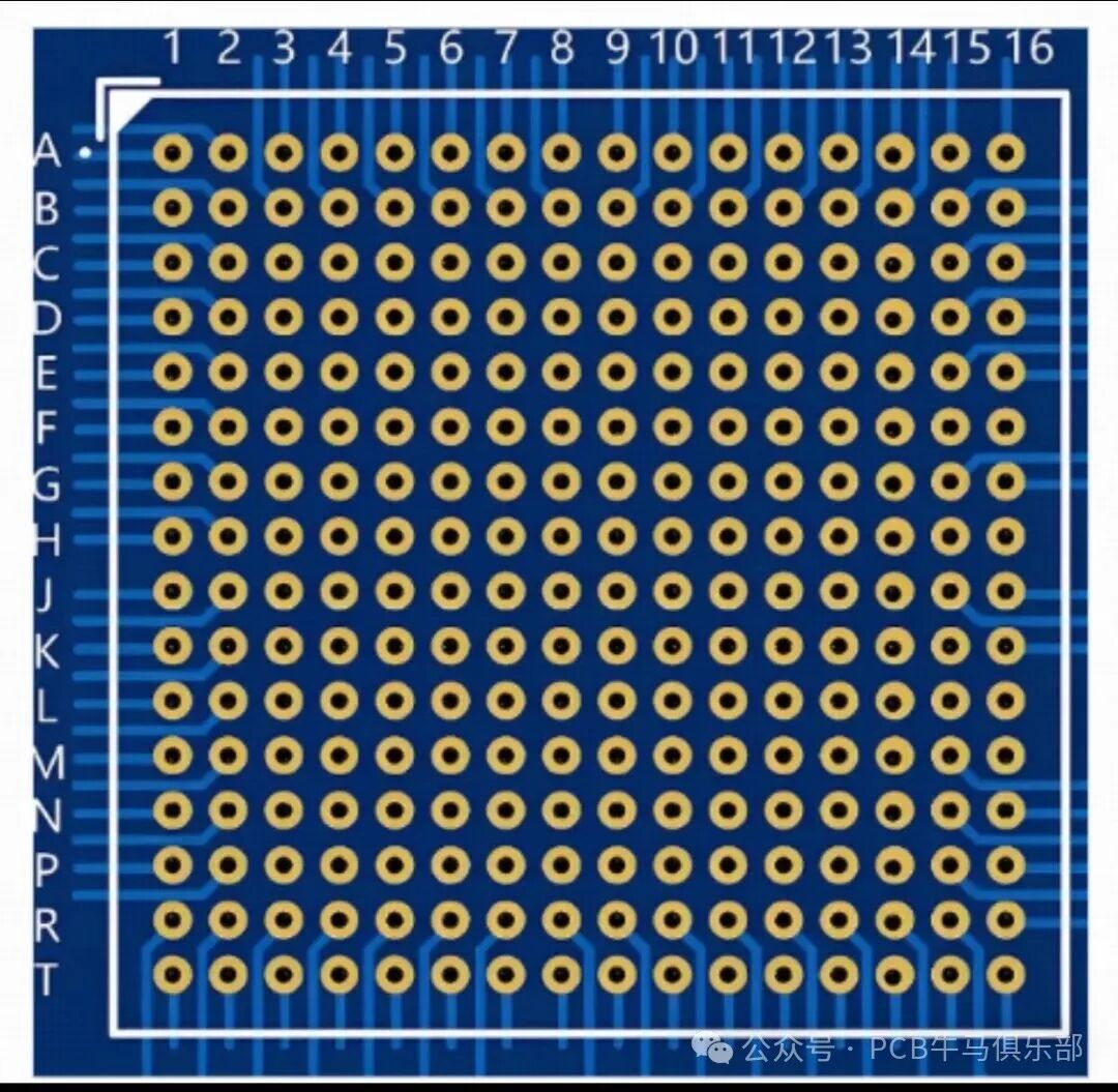
Microhole and Routing Technology: Laser processing is used to create microholes (<0.1mm) and fine traces (line width/spacing ≤3mil), reducing discontinuities in signal paths. Routing follows principles of equal length, equal spacing, and avoiding right angles (using arcs or 45° transitions) to minimize crosstalk and reflections.
3. Heat Management: The Guarantee of Overclocking Stability
The enormous power consumption brought by overclocking must be dissipated through an effective heat dissipation system. The PCB undertakes the dual task of conducting heat away from the chip (core) and the power module (VRM).
Thermal Management of PCB Materials:
High Thermal Conductivity Materials: Selecting substrates with higher thermal conductivity, such as certain ceramic-filled hydrocarbon boards, which can achieve thermal conductivity of 0.8W/m·K, and even enhance it to 5W/m·K through special designs (such as embedding copper blocks or heat pipes), far superior to ordinary FR-4.
Thick Copper Design: Using thick copper foil (such as 2oz, 3oz, or even 10oz) in power layers or areas requiring heat dissipation, utilizing copper’s high thermal conductivity as an internal “heat sink” to quickly and evenly conduct heat from localized hotspots.
PCB Structural Design for Heat Dissipation Optimization:
Thermal Via Arrays: Densely arranging metallized vias beneath chip pads or near power MOSFETs to quickly conduct heat from the top layer to the bottom layer or internal copper foil for heat dissipation.
* Large Area Copper Pour and Heat Dissipation Pads: Maximizing copper pour in non-routing areas of the PCB and connecting it to the ground network to form a large heat dissipation plane. The heat dissipation pads (Exposure Pads) of the chip must be reliably connected to large area copper foils in the inner or bottom layers through optimally designed via arrays.
* Composite Heat Dissipation Structures: High-end graphics cards and server motherboards often adopt solutions that directly integrate “copper substrates with embedded heat pipes” or “vapor chambers” with the PCB, making the PCB itself part of the heat dissipation system.
4. Hardware and Software Collaboration: Intelligent Overclocking
Hardware Coordination:
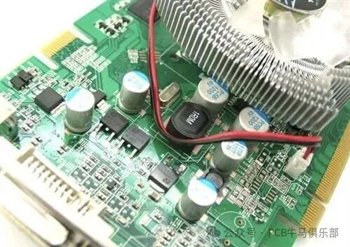
* Precision Power Supply Design (VRM): Overclocking requires extremely stable and precise voltage supply. Motherboards/GPUs use multi-phase power supply (such as 12+2 phases, 16+1 phases), with each phase equipped with high-quality DrMOS or GaN (Gallium Nitride) power devices, solid-state capacitors, and enclosed inductors to provide low ripple, high current power. PCB design must optimize the width and length of power paths to reduce impedance, ensuring minimal voltage drop before reaching the chip.
* Sensor Network: The PCB is equipped with temperature sensors (monitoring CPU/GPU cores, power modules, memory chip temperatures), voltage sensors, and current sensors to collect hardware status data in real-time.
Software/Firmware Coordination:
* BIOS/UEFI and Firmware: Provide user-friendly overclocking setup interfaces (such as Intel XTU, AMD Ryzen Master, and various motherboard manufacturers’ BIOS overclocking menus), allowing users to adjust multipliers, voltages, memory timings, and other parameters. The firmware is responsible for converting these settings into specific control instructions for hardware (such as clock generators and voltage regulation modules).
* Operating System-Level Tools and Drivers: Vendor-provided overclocking software (such as MSI Afterburner for GPU, ASUS AI Suite) allows for real-time adjustments and monitoring within the operating system. GPU drivers also include support and optimization for overclocking features.
* Dynamic Tuning and Protection: The software system dynamically adjusts fan speeds, core frequencies (such as Intel’s Turbo Boost Max 3.0, AMD’s Precision Boost) based on sensor feedback data, and automatically reduces frequency when detecting excessive temperatures or unstable voltages to protect hardware (Thermal Throttling). Some AI-driven overclocking tools (such as ASUS AI Overclocking) can even learn hardware characteristics and automatically find optimal overclocking parameters.
* Stability Testing Software: Tools like Prime95 (for CPU), FurMark (for GPU), and MemTest86 (for memory) are used to stress test the system after overclocking to verify its stability under high load.
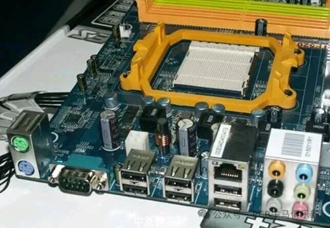
Collaborative Closed-Loop Example: A user sets the CPU core voltage to 1.3V and the multiplier to 50x (i.e., 5.0GHz) in the BIOS. The BIOS firmware sends this instruction to the voltage regulation module (VRM) and clock generator. The VRM outputs the precise 1.3V voltage according to the instruction, delivered through the PCB’s low-impedance power path to the CPU. While the CPU operates at 5.0GHz, its internal and PCB temperature sensors continuously monitor the temperature. Once the temperature approaches a safe threshold (e.g., 90°C), the monitoring software in the BIOS/operating system instructs the motherboard fan to speed up or commands the CPU to automatically reduce the multiplier (e.g., down to 48x) to lower power consumption and temperature, thus maintaining system stability. This entire process is the result of collaboration between hardware (PCB, VRM, sensors, CPU) and firmware/software (BIOS, drivers, monitoring programs).
Conclusion
When printed circuit boards were first invented, they were used in radios, and toys were used for conductivity. In the world of extreme performance overclocking, PCBs have evolved from a passive connection platform into an active participant that integrates high-frequency high-speed signal transmission, high current low-loss power supply, and efficient thermal management. By adopting low Dk/Df high-frequency high-speed materials, implementing precise manufacturing processes (hybrid lamination, impedance control, microhole technology), optimizing heat dissipation structural design, and deeply collaborating with advanced power supply hardware, intelligent BIOS/UEFI firmware, and operating system software, modern PCBs pave a solid, stable, and efficient “highway” and “heat dissipation channel” for the overclocking journey of core chips like CPUs and GPUs.
Note: The above discussion is for reference only and serves as a starting point for further exploration! Each factory’s chemicals/processes/equipment/product structures, etc., have various differences, and one must not rigidly apply experiences directly; all effective improvement measures come from experimental data! As a professional quality of engineering technicians, one must “speak with data.”
This public account will continue to update information related to PCB manufacturing and cutting-edge technologies.
Thank you for being not only good-looking and handsome but also able to move your golden fingers to make money. Please follow, collect, like, share, and leave comments!!!
Original content is not easy; if you want to reprint, please privately message the author, obtain consent, and indicate the source before reprinting. Thank you for your cooperation!