
In embedded development, many students encounter signal integrity issues. If the signal is not complete, it can lead to data loss, errors, and even problems with system performance and reliability. So how can we ensure signal integrity in PCB development?
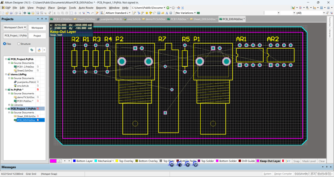
 01Reasonable Layout Planning
Functional Partitioning
-
Dividing the circuit board into functional zones is the foundation for ensuring signal integrity. Separate analog circuits, digital circuits, and power circuits into different areas.
-
For high-speed signal sections, such as DDR (Double Data Rate) memory interface circuits or high-speed communication circuits, they should also be separately partitioned and kept at a certain distance from other low-speed signal areas. This can avoid crosstalk caused by electromagnetic fields generated during high-speed signal transmission.
Component Placement in Functional Partitioning
-
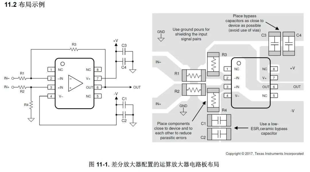
The placement of key components directly affects the signal path. For signal source and receiving components, try to shorten the distance between them to reduce signal transmission delay.
-
The pins of high-speed signal driver chips and receiver chips should be as close as possible to reduce the length of the signal transmission line. At the same time, avoid placing high-speed signal pins near components that may cause interference, such as clock generators and high-power chips.
 02Correct Wiring Rules Setting
Line Width Control
-
Determine the line width based on the current size of the signal. Generally, power and ground lines require wider widths to carry larger currents, reducing the resistance and voltage drop of the line.
Spacing Rules
-
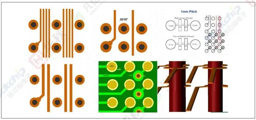
The spacing between lines on different signal layers and within the same signal layer must be sufficient. The size of the spacing depends on the signal voltage, the dielectric strength of the insulating material, and the PCB manufacturing process.
-
When considering high-speed signals, special attention should be paid to crosstalk issues. Crosstalk is the phenomenon where a signal on one line interferes with adjacent lines through electromagnetic coupling. To reduce crosstalk, the spacing between high-speed signals should be appropriately increased; it is generally recommended that when the signal transmission rate is high (e.g., greater than 1GHz), the spacing should not be less than 1/10 of the signal wavelength.
Wiring Topology Structure Selection
-
Common wiring topology structures include Daisy-Chain, Star, and Tree. For clock signals and other high-speed signals with strict timing requirements, a star topology should be adopted as much as possible.
 03Impedance Matching
Transmission Line Theory Basics
-
In high-speed signal transmission, PCB traces can be regarded as transmission lines. According to transmission line theory, when signals are transmitted on a transmission line, if the characteristic impedance of the transmission line does not match the impedance of the signal source and load, reflections will occur. Reflected signals will superimpose with the original signal, leading to signal distortion. Therefore, it is necessary to ensure that the characteristic impedance of the transmission line matches the impedance of the signal source and load for reflection-free signal transmission.
Matching Methods
-
Terminal matching is a common impedance matching method. Connecting a resistor equal to the characteristic impedance of the transmission line at the end of the signal transmission line can absorb reflected signals and avoid their generation.
-
Source matching is also an effective method. By placing a resistor in series at the signal source end, the output impedance of the signal source can match the characteristic impedance of the transmission line. This method can reduce reflections at the source end but may reduce the signal’s driving capability, requiring a trade-off based on the actual situation.

04Power Integrity Design
Use of Decoupling Capacitors
-
Decoupling capacitors should be placed near the power pins of each chip. Decoupling capacitors can provide local high-frequency current to the chip, reducing the impact of power fluctuations on the chip.
Design of Power and Ground Planes
-
When using multilayer PCB design, try to use complete power and ground planes. Power and ground planes can provide low-impedance power and ground return paths, reducing power noise. For example, in a four-layer PCB, the top and bottom layers are used for signal routing, while the middle two layers serve as power and ground planes.
05Signal Shielding and Protection Design
Use of Shielding Covers
-
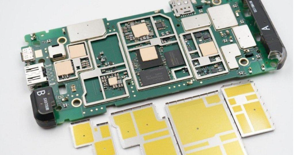
For sensitive signals that are easily affected by external electromagnetic interference or parts that generate strong electromagnetic radiation, metal shielding covers can be used.
-
The grounding of the shielding cover is crucial. The shielding cover should be well connected to the PCB ground plane to ensure that electromagnetic interference signals can be effectively grounded. The number and location of grounding connection points should be reasonably determined based on the size and shape of the shielding cover; generally, multiple grounding connection points are needed for larger shielding covers.
Protection Wiring
-
Grounding copper foil can be set around sensitive signal lines. Protection wiring serves to isolate and shield these lines.
 Exclusive for Fans
We have organized resources worth over 2000+

Content includes:
Software testing learning path from 0 to 1
Common testing templates and strategies in the workplace
Software testing improvement eBook
Classic interview questions
Songqin recorded classes
Limited time free~~~
 Long press the image below
Add teacher Tang Tang from Songqin to get resources for free

Currently, over 100,000 people have followed and joined us


Long press the QR code
Follow the 【Songqin Online Course】 video account