
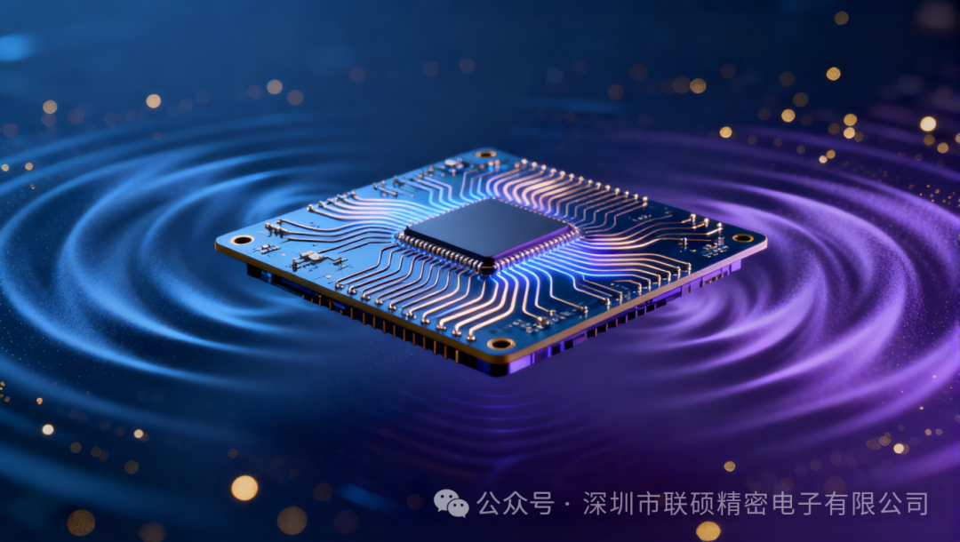
In the rapid development of 5G communication, millimeter-wave radar, and IoT devices, the design quality of RF PCBs, which are the core of signal transmission and processing, directly determines the performance boundaries of the entire system. Once regarded as a ‘black art’ reliant on experience, RF design often required engineers to go through repeated trial and error to find optimal solutions. However, as frequencies rise into the millimeter-wave and even terahertz domains, any slight deviation is dramatically amplified, making traditional methods unsustainable. A profound transformation from ’empirical art’ to ‘precision science’ is quietly occurring in the field of RF PCB design.
1. Core Challenges: The ‘Invisible’ Battlefield at High Frequencies
The operational stage of RF PCBs is the electromagnetic wave world at the GHz level. Here, the flow of current and the distribution of electric fields are distinctly different from low-frequency circuits, facing three core challenges:
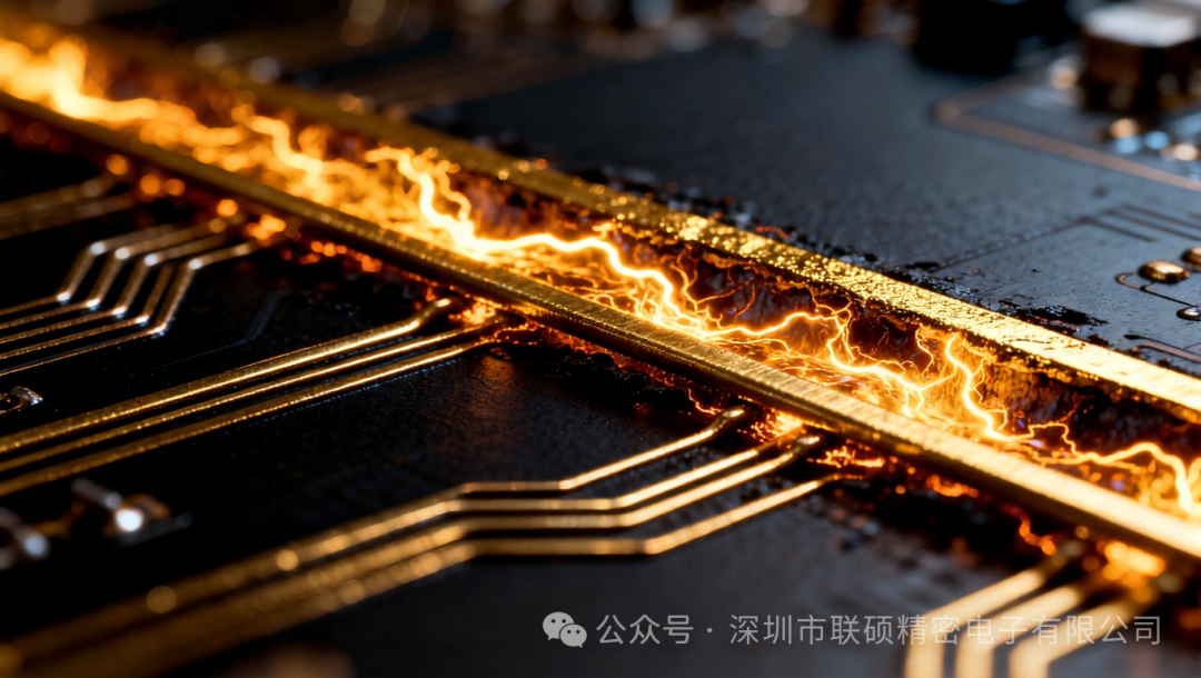
1. Stringent requirements for signal integrity: High-frequency signals exhibit significant ‘skin effect’ in transmission lines, where current is concentrated only at the surface of the conductor to a depth of microns. This means that subtle factors such as the surface roughness of copper foil and the purity of dielectric materials can directly translate into additional signal losses. Additionally, when the length of the transmission line is comparable to the signal wavelength, standing waves and reflections occur, leading to severe signal distortion. For example, in the 28GHz 5G millimeter-wave band, the wavelength is only about 10.7 mm, requiring control of trace lengths to sub-millimeter precision.
2. The complex game of electromagnetic compatibility: The RF board itself is both a source of signal transmission and a susceptible receiver. Noise generated by digital circuits and power modules on the board can easily couple into sensitive RF receiving paths, causing a decrease in reception sensitivity; electromagnetic interference from the external environment is also pervasive. Establishing clear ‘electromagnetic boundaries’ for circuits with different characteristics and power levels within a compact board space is fundamental to achieving stable communication.
3. Collaborative design for thermal management: High-power amplifiers and other devices generate significant heat during operation. Poor heat dissipation can lead not only to performance drift but also to shortened component lifespan. Thermal management and electromagnetic design must be coordinated; for instance, the arrangement of heat dissipation vias must consider thermal conductivity while not compromising the integrity of ground planes or introducing additional parasitic inductance.
2. Breaking the Deadlock: Precision Control Across Three Design Dimensions
To address the aforementioned challenges, the design philosophy must elevate from ‘just connecting’ to ‘controlling electromagnetic waves’, focusing on three dimensions:
1. Precise impedance control and routing artistry: Impedance matching is the lifeline of RF design. The goal is to strictly control the characteristic impedance of transmission lines to standard values such as 50Ω or 75Ω. This requires precise calculations of the relationships between dielectric thickness, copper foil thickness, and trace width, ensuring continuity of impedance along the entire path from chip pins to antenna ports. During routing, the principle of ‘short and straight’ should be followed, avoiding sharp corners and using arcs or chamfers for smooth transitions to minimize reflections. For critical differential pairs, strict ‘equal length, equal spacing, equal width’ layouts are required to ensure common-mode rejection capability.
2. Partitioned and layered electromagnetic isolation strategies: Successful RF layout begins with reasonable ‘functional partitioning’. Typically, a ‘linear’ or ‘L-shaped’ layout is used to clearly separate different functional circuit modules such as RF reception, transmission, local oscillation, and digital control, with physical isolation provided by grounding shields or via walls. In layered design, having a complete ground plane adjacent to high-frequency signal layers is key to providing low-impedance return paths and suppressing radiation. This ‘partitioned design and layered shielding’ strategy is akin to setting up soundproof rehearsal rooms for different sections of musicians, ensuring overall harmony.
3. Selection of special materials and processes for high frequencies: Ordinary FR-4 materials experience a sharp increase in loss above 1GHz, failing to meet high-performance requirements. Therefore, special high-frequency materials such as Rogers and Taconic are often selected, which have more stable and lower dielectric constants and loss factors. In terms of processes, priority should be given to blind and buried vias to reduce the impact of parasitic parameters from through-holes; control over soldering processes must also be particularly meticulous to avoid excess solder forming unintended RF components.
3. Future Trends: Simulation-Driven and Intelligent Integration
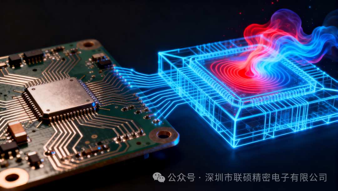
As operating frequencies continue to rise, RF PCB design increasingly relies on advanced electromagnetic simulation tools. Engineers can predict signal S-parameters, radiation field patterns, and thermal distributions during the design phase using simulation software, allowing them to identify and resolve potential issues in advance, liberating the design cycle from the ‘design-sample-test-modify’ loop to achieve ‘right the first time’. Looking ahead, system-in-package (SiP) technology will integrate RF front-ends, passive components, and even antennas into a single package, significantly reducing board-level interconnection losses and space. At the same time, artificial intelligence is beginning to assist in topology optimization and parameter tuning. RF PCBs are no longer just substrates for components; they are evolving into ‘subsurface functional structures’ that integrate transmission, filtering, and radiation functions, raising higher demands on engineers’ multi-physical field collaborative design capabilities.
RF PCB design, once a profound skill, is shedding its mysterious veil under the empowerment of digital and modeling tools, evolving into a quantifiable and predictable precision science. For enterprises and engineers, only by actively embracing this trend, deeply understanding the essence of electromagnetism, and mastering advanced design and simulation tools can they build a solid hardware foundation with excellent performance and reliability in the high-frequency, high-speed competitive wave, ultimately harnessing the omnipresent electromagnetic waves.
Follow [LianShuo Circuits] for more:
Click to follow for more stable designs and smoother debugging!
(For more professional content on circuit boards, feel free to click“Read the original text” for reference.)