1. Analysis of Google TPUv7 and OCS Technology Architecture1.1 Core Technological Breakthroughs of TPUv7 (Ironwood)Google officially released the seventh generation TPU chip Ironwood in April 2025, marking a significant breakthrough in AI computing power technology. This chip achieves a peak computing power of 4614 TFLOPs (FP8 precision) on a single chip, equipped with 192GB of HBM3e memory, a memory bandwidth of up to 7.4TB/s, and a power consumption of approximately 1000W. Compared to its predecessor, Ironwood’s computing power has increased by 4.7 times, with an energy efficiency ratio of 29.3 TFLOPs per watt, which is double that of the previous generation.
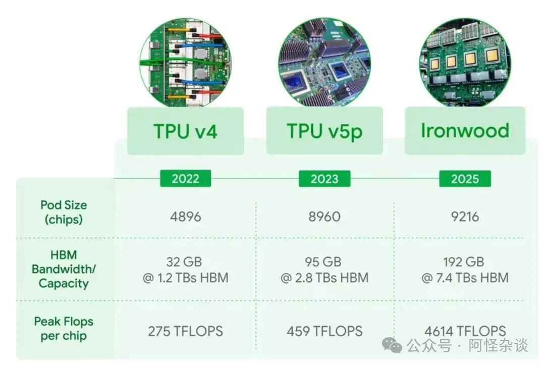
In terms of architectural design, Ironwood adopts an innovative Systolic Array design, supporting FP8 computing precision for the first time, while the previous generation only supported INT8 inference and BF16 training. This technological breakthrough enables Ironwood to handle large-scale language models and mixture of experts models with greater capability. The inter-chip interconnect (ICI) technology has also seen significant improvements, with a bidirectional bandwidth of 1.2Tbps, a 50% increase over the previous generation, supporting a deployment of 9216 chip clusters, with a total computing power of up to 42.5 Exaflops. The cluster architecture of Ironwood demonstrates remarkable scalability. When expanded to a Superpod configuration of 9216 chips, the total computing power reaches 42.5 Exaflops, more than 24 times that of the world’s largest supercomputer, El Capitan (1.7 Exaflops). This ultra-large-scale cluster is made possible by Google’s unique 3D Torus topology, where each logical unit is a 4×4×4 node array, achieving a network bandwidth of 1.8PB/s through InterChip Interconnect (ICI) technology.1.2 Advantages of OCS Optical Switching Technology ArchitectureOCS (Optical Circuit Switch) technology is a key technological innovation for Google to achieve ultra-large-scale TPU clusters. Unlike traditional “optical-electrical-optical” signal conversion, OCS completes signal routing directly in the optical domain, completely eliminating the bottleneck of optical-electrical conversion, achieving true “light-speed” data transmission.
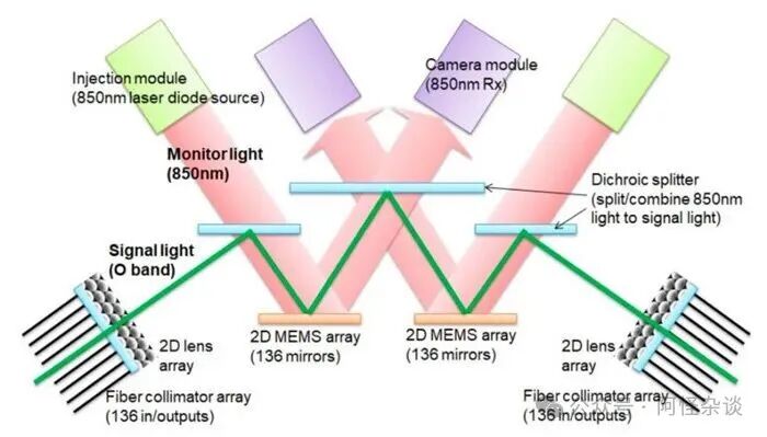
Illustration of OCS working principle: Intuitively shows how OCS works using two MEM arrays without the need for optical-to-electrical-to-optical conversion, thus saving power.
In the Ironwood cluster, 48 OCS switches connect 9216 TPU chips, creating a low-latency, high-bandwidth dynamic photonic network. The core advantages of OCS technology are reflected in four aspects: first, extremely low latency, with a single-hop delay of less than 1ns, significantly improving the training efficiency of tens of thousands of GPUs/TPUs; second, controllable power consumption, reducing power consumption by 50%-70% compared to traditional electrical switching; third, strong performance, with a single fiber bandwidth exceeding 100Tbps, and a single OCS supporting 128-320 optical ports; finally, cost optimization, allowing Google to reduce capital expenditures by 30%. OCS technology employs various implementation solutions, with the MEMS (Micro-Electro-Mechanical Systems) solution dominating the market, accounting for over 70%. The MEMS solution controls optical path switching by adjusting the angle of miniature mirrors, with each small mirror equipped with a two-dimensional (X/Y axis) pivot and dedicated control system, ensuring mature technology, balanced performance, and port expansion up to 320×320, with a switching speed of milliseconds and a cost of about $50,000 per unit. Another DRC (Silicon-based Liquid Crystal) solution adopts a fully solid-state design with no moving parts, achieving optical path refraction by controlling the structural changes of liquid crystal molecules, with a lifespan about ten times that of MEMS (over 10 years), and a slightly lower cost (about $40,000 per unit), but slower switching speed.1.3 Performance Comparison with Competitors like NVIDIA GB200Compared to NVIDIA’s latest Blackwell B200 chip, TPUv7 forms a balanced competitive landscape in key performance indicators. In terms of FP8 computing power, TPUv7 reaches 4.6 petaFLOPS, slightly higher than B200’s 4.5 petaFLOPS, but slightly lower than GB200 and GB300’s 5 petaFLOPS. In memory configuration, both are equipped with 192GB of HBM memory, with TPUv7’s bandwidth at 7.4TB/s, slightly lower than B200’s 8TB/s.
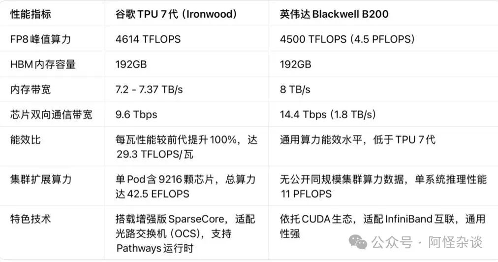
At the system level, there are significant differences in architectural design philosophy between the two. NVIDIA’s GB200 adopts a traditional switch connection method, capable of connecting up to 72 chips, offering greater flexibility; while TPUv7 employs a 3D toroidal topology and OCS optical switching technology, allowing a single cluster to scale up to 9216 chips, providing a clear advantage in ultra-large-scale deployment. In terms of power consumption, TPUv7’s power consumption is approximately 1000W, lower than GB200’s approximately 1200W, giving it an advantage in energy efficiency. In practical application scenarios, TPUv7 is specifically optimized for AI inference, being Google’s first TPU designed for the “Inference Era.” Compared to the previous TPUv5p, Ironwood’s peak performance has increased tenfold; compared to TPUv6e, training and inference performance has improved fourfold. This specialized design gives TPUv7 a unique advantage in handling large-scale language model inference tasks.2. The Impact of Google’s Entry on the AI Computing Hardware Supply Chain2.1 Construction of TPU Chip Supply Chain SystemThe supply chain system for Google TPU exhibits a highly centralized characteristic, with TSMC as the exclusive wafer foundry occupying a core position. TPU v6/v7 is produced using TSMC’s 3nm process, requiring 4900 wafers per month for every 1GW of TPU capacity, corresponding to $1.895 billion in revenue, becoming a core growth point for TSMC’s advanced processes. According to the latest data, Google has reserved 90,000 wafers (TSMC 85,000 wafers, ASE/Siliconware 5,000 wafers), mainly for the production of TPU v6e and Ironwood. In terms of chip design, Google leads the overall architecture and functional definition, while Broadcom participates in some of the chip’s backend design work. Notably, Google is collaborating with MediaTek to develop the next generation TPU, with MediaTek responsible for managing the input/output modules for communication between the main processor and peripheral components, while Google will still handle most of the design work. The packaging and testing stages are mainly handled by manufacturers like ASE, using advanced CoWoS packaging technology. The main supplier of HBM memory is Samsung, providing HBM3e technology, with quarterly bit sales increasing by 80% year-on-year. Within the entire supply chain system, the profit margin for architecture design and ecosystem integration exceeds 50%, while the profit margin for foundry manufacturing, packaging, and testing is only 5%-15%.2.2 Explosive Demand for Optical Communication Industry ChainThe demand for optical communication hardware from Google TPU clusters is experiencing explosive growth. The procurement volume of 800G optical modules, as the core component of TPU clusters, has achieved an astonishing 27-fold increase within 2025. According to market forecasts, global demand for 800G optical modules is expected to double from approximately 9 million units in 2024 to 18 million units in 2025, with demand expected to reach 40 million units in 2026. Zhongji Xuchuang, as the largest supplier of 800G optical modules for Google, occupies 50%-60% of its procurement share, with shipments reaching 500,000 units in 2024 and expected to grow to 800,000 units in 2025. The company’s 1.6T optical module, which uses silicon photonics hybrid packaging technology, has been certified by Google, making it the exclusive supplier, with related order amounts exceeding 5 billion yuan in 2025, and a three-year long-term supply agreement signed. Zhongji Xuchuang’s 800G optical module yield rate reaches 95%, 10 percentage points higher than the industry average, with power consumption reduced by 20%, saving Google 30 kWh per module annually. Xinyi Sheng first entered Google’s 800G supply chain in 2025, achieving a supply share of 20%. The company’s 1.6T optical module, based on a 3nm DSP chip, has been certified by NVIDIA GB200, with small batch deliveries starting in Q2 2025, expected to contribute over 3 billion yuan in revenue in 2026. Xinyi Sheng’s 1.6T products have entered the supply chains of major clients like Meta and Google, with the value of each AI server’s supporting components increasing by over three times. The 1.6T optical module market is also rapidly developing. According to industry forecasts, demand for 1.6T modules is expected to be 3-5 million units in 2025, with prices being twice that of 800G. Both Zhongji Xuchuang and Xinyi Sheng’s 1.6T products have entered the sampling or mass production stage, expected to see large-scale volume in 2026.2.3 Performance of Optical Module Manufacturers Validating OrdersZhongji Xuchuang’s performance in Q3 2025 fully validates the strong pull effect of Google’s demand. Revenue from Google reached 3.2 billion yuan, a year-on-year increase of 65%, accounting for 12.8% of the company’s total revenue. In the first half of 2025, the gross profit margin of the company’s optical module business was 39.96%, significantly up from 33.83% in the same period last year, with the notable increase in gross margin mainly due to the rapid increase in the shipment proportion of high-end optical modules like 800G. In terms of order elasticity, Google is expected to ship 3.5 million TPU V7 units in 2026, corresponding to a demand for over 60 million optical modules. Based on Zhongji Xuchuang’s 50%-60% share, it could contribute over 36 million orders. The company’s current 1.6T optical module capacity has reached 150,000 units per month, and it has achieved localized delivery through its Texas factory, mitigating supply chain risks, with revenue from Google expected to increase to 35% in 2025. Xinyi Sheng, as the second-largest supplier of optical modules for Google, achieved its first batch supply to Google in 2025. The company’s 800G optical module revenue accounts for over 67%, and the comprehensive upgrade of its product structure has driven an increase in profitability. With the mass production of 1.6T products and the continuous growth of Google orders, Xinyi Sheng is expected to achieve further breakthroughs in performance in 2026.2.4 Orders from Core Component Suppliers of OCSCore component suppliers for OCS optical switches are also experiencing an order explosion. Tengjing Technology provides high-precision optical components for Google’s OCS switches, including refractive prisms, circulators, and other core devices, with a single device value of $700-750, accounting for 15% of the total machine cost. The company holds over 60% of the global market share for vanadium oxide crystals and 40% for WSS filters, exclusively supplying Google’s TPU clusters through Coherent. In 2025, it is expected to supply 20,000 OCS devices to Google, corresponding to revenue of approximately 150 million yuan. Juguang Technology provides two-dimensional micro-lens arrays for OCS switches, with specifications of 276 channels, priced at $1 per channel, with a single machine value of approximately $276. The company acquired Swiss SMO, gaining the ability to supply key optical components such as high-precision lens arrays, with its micro-lens arrays capable of compressing light spots to 50 microns, directly applied in Calient’s high-density OCS solutions. Guangku Technology became the core foundry for Google’s OCS switches after acquiring Wuhan Jiepai (later renamed Wuhan Guangku) in June 2025, with a foundry share exceeding 70%. Wuhan Jiepai was previously the exclusive foundry for Google’s OCS switches, possessing mature MEMS solution manufacturing capabilities. Guangku Technology collaborated with Calient to develop MEMS solution OCS switch products, adopting MEMS micro-mirror technology to achieve a 64×64 port scale, meeting Google’s 1.6T optical module requirements. Dekeli, as Google’s only optical waveguide solution supplier, has a silicon-based optical waveguide OCS solution with nanosecond-level delay (traditional MEMS is microsecond-level) and 80% lower power consumption. In July 2025, Dekeli passed single-machine verification and received an order for 10 sample units, priced at $250,000 per unit, with plans for delivery by the end of 2025. The company is advancing to the second generation of high-dimensional OCS development, aiming to launch a prototype in the first half of 2026.3. Breakthrough Paths for Domestic Hardware Manufacturers and Increasing Localization Rate3.1 Analysis of Localization Rate Increase TrendsChinese companies are undergoing a historic change in their position within Google’s TPU supply chain, with the localization rate showing rapid improvement. According to the latest data, the localization rate of domestic enterprises in the high-end hardware sector has increased from 15% to 35%. This improvement is particularly evident in several key areas: the localization rate in the MEMS chip sector exceeds 15%, in optical devices it reaches 20%-30%, and in the complete machine foundry segment is about 18%. In the optical module sector, localization achievements are particularly significant. In the 2024 global top 10 optical module manufacturers list, Chinese manufacturers occupy 7 seats, with a combined market share exceeding 70%, completely changing the previous dominance of Japanese and American manufacturers. Companies like Zhongji Xuchuang, Xinyi Sheng, and Huagong Technology have not only achieved mass supply in 800G products but have also made technological breakthroughs in next-generation products like 1.6T. Google’s localization strategy for its supply chain is also accelerating. According to the latest information, Google plans to increase the localization ratio of its supply chain from the current 5% to 20% by 2026. This strategic adjustment provides more opportunities for Chinese companies to enter the core supply chain, especially in supporting areas such as PCB, power supplies, and structural components. From a segmented perspective, the localization process shows differentiated characteristics. In fields with relatively low technical barriers, such as passive components, PCBs, and power supplies, the localization rate is increasing rapidly; in technology-intensive areas like optical modules and core OCS components, although starting later, rapid progress is being made through technological innovation and mergers and acquisitions, catching up with international advanced levels.3.2 Breakthrough Cases of Guangku Technology and DekeliGuangku Technology achieved a significant breakthrough in Google’s OCS supply chain through strategic acquisitions. In June 2025, Guangku Technology acquired Wuhan Jiepai, which was previously the exclusive foundry for Google’s OCS switches. Through this acquisition, Guangku Technology not only gained mature MEMS solution manufacturing capabilities but also inherited a deep cooperative relationship with Google. Currently, Guangku Technology holds over 70% of the foundry share for Google’s OCS, becoming a core supplier. The company’s technical integration capabilities are also noteworthy. The company possesses FAU (Fiber Array Unit) technology, which can synergize with Jiepai’s foundry business. In a single OCS, the FAU component value reaches $30,000, significantly enhancing the company’s value share in the supply chain. The company has also collaborated with Calient to develop MEMS solution OCS switch products, adopting MEMS micro-mirror technology to achieve a 64×64 port scale, with technical indicators reaching international advanced levels. Dekeli’s breakthrough lies in its technological innovation. As Google’s only optical waveguide solution supplier, Dekeli’s silicon-based optical waveguide technology has revolutionary advantages over traditional MEMS solutions: delays as low as nanoseconds (traditional MEMS are microseconds), 80% lower power consumption, and a 30% increase in transmission efficiency. The company’s self-developed “Photon Routing Engine” compresses the routing delay of optical signals to 10 microseconds, only 1/10 of traditional solutions. Dekeli’s technological breakthroughs have received high recognition from Google. In July 2025, the company passed single-machine verification and received an order for 10 sample units, priced at $250,000 per unit, fully reflecting its technological premium capability. More importantly, Dekeli’s solution has captured over 60% of the share in Google’s new data center clusters, demonstrating strong market competitiveness. The company is advancing the development of the second generation of high-dimensional OCS, aiming to launch a prototype in the first half of 2026, further consolidating its technological leadership.3.3 Breakthroughs of Other Domestic Manufacturers in the Supply ChainIn addition to Guangku Technology and Dekeli, several Chinese companies have achieved significant breakthroughs in Google’s TPU supply chain. In the PCB sector, Huidian Co. has become the core supplier of PCBs for Google TPU, accounting for about 30% of Google’s share, leading the production of 30-40 layer boards; Shenzhen South Circuit supplies the 44-layer board for TPU V7, being the exclusive supplier for this high-spec PCB; Shenghong Technology is the main supplier for V6/V7 versions and is also the largest global supplier of Google’s data center UBB (Universal Base Board). In the power supply sector, Xinle Energy has successfully entered Google’s TPU power supply chain, providing secondary and tertiary power modules, with overall intended orders exceeding $500 million, becoming one of the few domestic power suppliers certified by Google. In the packaging sector, Industrial Fulian is a core partner for Google’s TPU packaging foundry, with orders from Google in Q2 2025 increasing by 150% year-on-year. The company’s newly established TPU packaging production line in Vietnam has a capacity of 200,000 units per month, providing capacity assurance for Google’s large-scale mass production of TPUs. In the optical communication sector, in addition to Zhongji Xuchuang and Xinyi Sheng, Huagong Technology’s cooperation with Google deeply covers three core areas: optical module supply, quantum technology components, and AI computing infrastructure adaptation, directly binding its business to Google’s full-stack AI innovation (TPU chips + OCS optical switching + Gemini large model).3.4 Market Share Changes Driven by Technological InnovationThe increase in market share of Chinese companies in Google’s supply chain is fundamentally driven by continuous technological innovation. Taking optical modules as an example, Zhongji Xuchuang’s 800G product yield rate reaches 95%, 10 percentage points higher than the industry average, with power consumption reduced by 20%, these technological advantages directly translate into market competitiveness. In the 1.6T product line, Zhongji Xuchuang has become Google’s exclusive supplier by adopting silicon photonics hybrid packaging technology, establishing a technological barrier that ensures the stability of market share. In the OCS technology field, Dekeli has achieved differentiated competition through its silicon-based optical waveguide technology. Compared to traditional MEMS solutions, optical waveguide technology has significant advantages in key indicators such as delay, power consumption, and transmission efficiency, which has earned Dekeli the position of exclusive supplier. Mergers and acquisitions have also become an important means for Chinese companies to rapidly acquire technological capabilities and market share. Guangku Technology’s acquisition of Wuhan Jiepai not only provided mature manufacturing capabilities but also secured a deep cooperative relationship with Google and market access qualifications. This “buy technology + buy market” strategy has helped Chinese companies shorten the technology accumulation cycle and quickly enter the high-end market. In the long term, as the technological capabilities of Chinese companies continue to improve and Google’s localization strategy progresses, it is expected that by 2026, Chinese companies’ overall share in Google’s TPU supply chain will exceed 40%, and in some segments, it may even reach over 50%. Particularly in optical communication, PCB, and power supply sectors, Chinese companies have already gained the strength to compete with international giants.
4. Analysis of Synergistic Growth Effects of Supporting Hardware4.1 Surge in HBM Memory DemandHBM (High Bandwidth Memory), as a key supporting component for AI chips, is experiencing explosive growth in demand. The four major AI chip manufacturers—NVIDIA, AWS, Google, and AMD—account for 95% of global HBM demand, forming a highly concentrated demand pattern. Google’s HBM demand in 2025 is expected to reach 0.41B Gb, mainly driven by training needs for TPU v5 and v6 versions, with TPU v5 training demand around 0.47B Gb. Google’s HBM configuration shows a clear upgrade trend, moving from TPU v5’s HBM2e 8hi 6-stack (capacity 96GB) to TPU v6’s HBM3e 8hi 8-stack (capacity 192GB), doubling the memory capacity. According to Samsung’s forecast, Google’s total HBM demand will grow from 2.4 million units in 2024 to 2.8 million units in 2026, with TPU v7p alone expected to require 1.7 million units in 2026. The supply-demand imbalance in the HBM market has led to continuous price increases. The unit price of SK Hynix’s HBM4 has risen to $560, over 50% more expensive than the previous generation. More seriously, SK Hynix’s production capacity for 2026 has been fully booked, and Samsung has also stopped accepting new orders for DDR25. This tight supply situation is expected to continue until 2027, with SK Hynix predicting that demand for HBM memory chips will grow at a rate of 82% per year. From a supply chain perspective, global HBM production capacity is mainly monopolized by three giants: Samsung, SK Hynix, and Micron. Among them, SK Hynix holds over 60% of the market share, leading by a significant margin. In response to the sky-high orders from AI companies, these giants are massively expanding production. Samsung plans to invest 47.4 trillion won in facility construction in 2025, with 86% of the budget directed towards the semiconductor sector, focusing on expanding 1c DRAM production lines to meet HBM4 demand.4.2 Tianfu Communication’s High Gross Margin Verification in Optical Device PackagingTianfu Communication, as a leading enterprise in the optical device packaging field, demonstrates its high gross margin, reflecting its technological barriers and market position. The company’s silicon photonic engine gross margin exceeds 50%, significantly higher than the traditional optical device gross margin of 30%-40%. In 2024, the company’s passive business revenue reached 1.576 billion yuan, with a gross margin of 68.41%, serving clients including Huawei and ZTE. The high gross margin of Tianfu Communication is backed by its unique competitive advantages. The company achieves dual advantages of cost control and yield improvement through “engineer skillset integration + internal vertical industry chain integration.” For optical devices with a normal gross margin of around 35%, Tianfu has increased the gross margin to over 50% through technological innovation and process optimization. This combination of cost and technological advantages has made Tianfu a supplier for NVIDIA’s CPO (Co-Packaged Optics), securing this important order after Zhongji Xuchuang withdrew. In Google’s supply chain, Tianfu Communication’s 1.6T optical engine accounts for over 60% of Google’s demand, with a CPO market share exceeding 70%. The company’s products entered mass production in Q2 2025, with a yield rate exceeding 90% and a gross margin of 60%-70%, significantly higher than traditional optical devices. In Q3 2025, the company’s gross margin remained above 50%, fully validating its technological leadership in the high-end optical device field. Tianfu Communication’s success is not only reflected in high gross margins but also in its layout for next-generation technologies. The company continues to invest in cutting-edge fields such as silicon photonics and CPO technology, ensuring its technological advantage in future competition. As the scale of Google’s TPU clusters expands and the 1.6T optical modules are widely applied, Tianfu Communication is expected to receive more orders, further consolidating its market position.4.3 Shenghong Technology’s Dual Order Dividend in PCBShenghong Technology has achieved a dual layout with NVIDIA and Google in the AI computing PCB market, fully benefiting from the demand growth of these two computing giants. As a Tier 1 supplier for NVIDIA, Shenghong Technology occupies over 50% of the global share in supplying PCBs for its GB200/GB300 servers, while also supporting the entire range of gaming graphics cards and data center GPUs. In Q1 2025, NVIDIA-related orders accounted for 70% of Shenghong Technology’s business volume, with delivery amounts exceeding 2 billion yuan, directly driving the company’s net profit for the quarter to skyrocket to 921 million yuan, a year-on-year increase of 339%. In Google’s supply chain, Shenghong Technology’s position is equally important. The company is the largest global supplier of Google’s data center UBB (Universal Base Board), ranking first in market share. At the same time, Shenghong Technology provides a 30-layer HDI + orthogonal backplane solution for Google TPU V6/V7, being the largest supplier for the V7 version PCB. The value of Shenghong Technology in Google’s TPU supply chain is particularly prominent. The company exclusively supplies PCB substrates for Google’s TPU V6/V7 generation chips, with a single board value reaching 300% of NVIDIA’s similar products. This high value is not only reflected in the technical content of the products themselves but also in their critical role in the overall TPU system performance. The company’s 8-layer 28-layer HDI technology has passed Google’s TPU orthogonal backplane certification, with technical indicators reaching international leading levels. Looking ahead, Shenghong Technology’s order prospects are very optimistic. The company has been confirmed as the core supplier for NVIDIA’s Rubin architecture PCB, and there are even reports that its 2027 production capacity has been pre-booked by NVIDIA. Meanwhile, with the expansion of Google’s TPU cluster scale and the launch of new generation products, Shenghong Technology is expected to receive more orders from Google. This dual order dividend provides strong momentum for the company’s continued growth.4.4 Opportunities for Other Supporting Hardware ManufacturersIn addition to HBM, optical device packaging, and PCBs, the construction of Google’s TPU clusters has also driven the development of multiple supporting hardware fields. In the power supply sector, Xinle Energy has successfully entered Google’s TPU power supply chain, providing secondary and tertiary power modules, with overall intended orders exceeding $500 million. As one of the few domestic power suppliers certified by Google, Xinle Energy’s success reflects the progress of Chinese companies in power supply technology. In the cooling sector, liquid cooling technology has become standard for AI servers. According to institutions’ forecasts, the global liquid cooling penetration rate is expected to exceed 30% by 2026, with a market size reaching tens of billions of dollars. The liquid cooling system used in Google’s TPU clusters poses higher requirements for high-performance cooling solutions, providing significant market opportunities for liquid cooling equipment manufacturers. In the structural components and connectors sector, with the expansion of TPU cluster scale, the demand for high-reliability, high-density connectors is rapidly growing. For example, suppliers of key components like MPO connectors have obtained about 10% of Google’s procurement share. These seemingly inconspicuous components actually have a significant impact on the stability and performance of the entire system. In the storage sector, although HBM occupies most of the attention, the demand for traditional storage devices is also increasing. TPU clusters require a large number of storage devices to support training and inference tasks, providing new growth points for SSDs, hard drives, and other storage device manufacturers. Especially in AI training scenarios, the demand for high-bandwidth, low-latency storage is particularly urgent. Overall, the construction of Google’s TPU clusters has formed a vast industrial ecosystem. In addition to direct chip and optical module suppliers, numerous supporting hardware manufacturers are involved. This comprehensive demand pull not only brings order growth to related enterprises but also drives technological progress and industrial upgrading across the entire hardware industry. As AI applications continue to deepen and the scale of TPU clusters continues to expand, opportunities in the supporting hardware field will continue to grow.
5. Restructuring of Market Landscape and Future Trend Predictions5.1 The Impact of Google’s Entry on the AI Computing Market LandscapeGoogle’s strong entry with TPUv7 and OCS technology is reshaping the global AI computing market landscape. The most direct impact is the challenge to the traditional GPU monopoly. NVIDIA, as the absolute leader in the AI chip market, is facing substantial challenges from dedicated AI accelerators for the first time. Google has not only achieved breakthroughs in technology but, more importantly, through the “TPU@Premises” program, has broken the limitation of needing to use TPU in Google Cloud, allowing customers to deploy TPU directly in their own data centers, a strategy that is highly disruptive. The market competition landscape is evolving from “one strong, many strong” to a “tripartite balance.” In addition to NVIDIA and Google, AMD is also accelerating its catch-up with its MI300 series products. More importantly, major cloud service providers are developing their own AI chips, such as AWS’s Trainium/Inferentia and Microsoft’s Maia GPU, forming a diversified competitive landscape. The fundamental reason for this change in landscape is that as AI applications develop deeply, the demand for computing power in different scenarios presents differentiated characteristics, making a single architecture insufficient to meet all needs. From the trend of market share changes, Google is rapidly eating into NVIDIA’s market share. According to the latest news, Meta is discussing a multi-billion dollar procurement of Google TPU, planning to deploy it on a large scale in its data centers by 2027, while also considering renting TPU computing power from Google Cloud in 2026. This news directly caused NVIDIA’s stock price to drop before the market on November 25, 2025, with a market value evaporating by $350 billion. Anthropic has also announced an unprecedented procurement plan to purchase up to 1 million TPU chips, with a transaction amount reaching hundreds of billions of dollars. From the evolution of technological routes, Google’s OCS optical switching technology is leading industry transformation. Traditional electrical switching architectures encounter bottlenecks when facing ultra-large-scale clusters, while OCS technology achieves low-latency, high-bandwidth, and low-power data transmission by eliminating optical-electrical conversion. This technological innovation not only enhances the performance of TPU clusters but also points the way for the entire industry’s technological development. It is expected that more manufacturers will adopt optical switching technology in the future, promoting the upgrade and replacement of the entire AI infrastructure.5.2 Changes in Procurement Strategies of Companies like Meta and AnthropicProcurement strategies of AI giants like Meta and Anthropic are undergoing fundamental changes, shifting from a single reliance on NVIDIA GPUs to a diversified procurement strategy. This shift is driven by multiple factors: first, supply chain security considerations, as over-reliance on a single supplier poses risks of supply interruption; second, cost pressures, as the explosive growth in AI training demand makes it essential to seek more cost-effective solutions; third, the diversification of technological needs, as different AI applications require various technical routes to support them. Anthropic’s procurement decisions are the most representative. As a major competitor to OpenAI, Anthropic announced a purchase of 1 million TPU chips from Google, an unprecedented order scale. According to Anthropic’s plan, these TPUs will be deployed in 2026, forming a computing power cluster exceeding 1GW. This is not only a large-scale procurement but also represents a significant shift in AI companies’ computing power strategies. By adopting TPU, Anthropic can gain a technological advantage that differentiates it from OpenAI while reducing its dependence on NVIDIA. Meta’s strategy is more complex and cautious. As the world’s largest social media company, Meta has enormous and diverse computing power needs. The company is negotiating with Google for a multi-billion dollar TPU deployment in 2027 while also evaluating other options. Meta’s strategy reflects the typical characteristics of large companies: not putting all eggs in one basket but diversifying procurement to spread risks and optimize costs. Notably, Meta is also developing its own AI chip, MTIA, indicating an intention to further reduce external dependencies. This change in procurement strategy has profound implications for the entire supply chain. For NVIDIA, while it still holds a dominant position in the short term, long-term growth faces challenges. The company needs to maintain its market position through technological innovation and ecosystem building, such as launching more powerful GB300 chips and strengthening software ecosystem development. For Google, this is a historic opportunity, opening up a vast market space through TPU. For other chip manufacturers like AMD and Intel, this is an opportunity for reshuffling, allowing them to gain more market share through differentiated strategies. From a longer-term perspective, this trend of diversified procurement will drive innovation and development across the entire AI chip industry. Manufacturers need to continuously enhance their technological capabilities, reduce costs, and optimize ecosystems to survive and thrive in fierce competition. This is beneficial for the entire industry and end users, leading to more innovations, better products, and more reasonable prices.5.3 2025-2026 AI Computing Hardware Market Growth ForecastAccording to predictions from several authoritative institutions, 2025-2026 will be an explosive period for the AI computing hardware market. TrendForce predicts that global AI server shipments will increase by over 20% annually in 2026, with the proportion of AI servers in the overall server market rising to 17%. Morgan Stanley defines 2026 as a “key year for explosive growth in AI technology hardware,” expecting the demand for AI server cabinets to surge from 28,000 units in 2025 to at least 60,000 units in 2026, achieving over a doubling in growth. In terms of market size, the growth prospects are even more astonishing. The global AI computing market size is expected to reach $1.21 trillion in 2025, a year-on-year increase of 35.9%. From 2025 to 2030, the global AI computing market size is expected to grow from $1.2 trillion to $5.8 trillion, with a compound annual growth rate of 37.6%. Gartner predicts that global AI spending will approach $1.5 trillion in 2025 and exceed $2 trillion in 2026. In the segmented market, the AI server market is experiencing particularly rapid growth. The global high-end AI server shipment volume is expected to grow from 639,000 units in 2024 to 1,323,000 units in 2025, nearly doubling. Among them, ultra-large-scale data center operators will be the main customers, with their demand for AI servers showing exponential growth. The optical communication market also has broad prospects. According to forecasts, global Ethernet optical module sales growth will reach 32% in 2025, with shipments of 800G DR8/FR8 being adjusted upward by 10%, and an additional $500-600 million in urgent orders for 1.6T. By 2026, it is expected that there will be a demand for 40 million 800G optical modules and 7 million 1.6T optical modules. From a regional distribution perspective, the growth of the Chinese market is particularly strong. In the short term (2025-2026), the global AI computing annual growth rate is expected to be 30%-50%, while China’s growth rate leads at 43%-74%. This high growth is mainly attributed to China’s advantages in AI application implementation, policy support, and industrial foundation. From a technological evolution perspective, several key trends are worth noting: first, the continuous improvement of computing power density, with single-chip computing power constantly increasing; second, the expansion of system scale, evolving from tens of thousands of card clusters to hundreds of thousands of card clusters; third, innovations in interconnect technology, with optical switching technology gradually becoming mainstream; fourth, optimization of energy efficiency ratios, focusing more on energy consumption control while pursuing high performance. Behind these growth forecasts is the comprehensive explosion of AI applications. From large language models to multimodal AI, from generative AI to inferential AI, various applications are rapidly increasing their demand for computing power. Especially as AI moves from the laboratory to industrial applications, the demand for computing power presents diversified and large-scale characteristics. This explosion of demand brings unprecedented development opportunities for the entire AI hardware industry chain.
6. Conclusion and Investment RecommendationsGoogle’s strong entry into the AI computing competition with TPUv7 and OCS optical switching technology marks a new development stage for the global AI hardware industry. Through a comprehensive analysis of technological architecture, supply chain impacts, localization processes, supporting industry synergies, and changes in market landscape, we can draw the following core conclusions: On the technology front, Google TPUv7 has reached or is close to NVIDIA GB200 levels in key indicators such as computing power, memory, and interconnect, particularly showing significant advantages in ultra-large-scale cluster expansion capabilities. The introduction of OCS optical switching technology not only addresses the bottleneck issues of traditional electrical switching but also points the way for technological development in the entire industry. This technological breakthrough has earned Google a place in the AI computing market and has driven technological progress across the entire industry. In terms of supply chain impacts, Google’s entry has brought multiple benefits. The direct effect is the explosive demand for core hardware such as optical modules, OCS devices, and HBM memory, with the 27-fold annual growth of 800G optical modules clearly demonstrating this strong pull effect. The indirect effect is the promotion of global supply chain layout and localization processes, providing historic opportunities for Chinese companies. The trend of increasing localization rates from 15% to 35% reflects the significant progress of Chinese companies in technological innovation and market expansion. The market landscape is undergoing profound changes. The shift from “one strong, many strong” to a diversified competitive landscape not only provides users with more choices but also drives innovation vitality across the entire industry. The diversified procurement strategies of companies like Meta and Anthropic reflect the market’s emphasis on technological diversity and supply chain security. It is expected that this trend will further strengthen in 2026, pushing the AI hardware market into a more open and fiercely competitive new stage. Based on the above analysis, we propose the following investment recommendations: Focus on the optical communication industry chain. As optical modules are key components of AI computing, they have the highest certainty of benefiting. It is recommended to focus on companies that have entered Google’s supply chain and occupy important shares, such as Zhongji Xuchuang (leader in 800G/1.6T optical modules), Xinyi Sheng (core supplier of 800G optical modules), and Tianfu Communication (high gross margin optical device packaging target). Also, pay attention to core component suppliers of OCS, such as Tengjing Technology (core components like circulators) and Juguang Technology (micro-lens arrays). Lay out opportunities for domestic substitution. With the continuous increase in localization rates, it is recommended to focus on companies that have achieved breakthroughs in key technology areas. Guangku Technology, which has become a core foundry for OCS through acquisitions, and Dekeli, as the exclusive optical waveguide solution supplier, both have high investment value. In the PCB sector, companies like Shenghong Technology, Huidian Co., and Shenzhen South Circuit that have entered Google’s supply chain are worth paying attention to. Seize opportunities in supporting hardware. The explosive demand for HBM memory brings opportunities to the related industry chain, although domestic companies have limited direct participation, upstream material and equipment suppliers can be focused on. There are also structural opportunities in supporting fields such as liquid cooling, power supplies, and connectors, such as Xinle Energy (power modules). Focus on technology innovation-driven companies. In the context of rapid iteration of AI hardware, technological innovation capability is key to long-term competitiveness. It is recommended to focus on companies with layouts in cutting-edge fields such as silicon photonics, CPO technology, and new packaging technologies, such as Huagong Technology. Risk warning: Attention should be paid to risks of technological iteration, supply chain fluctuations, and intensified market competition. Especially considering the rapid changes in the AI hardware market, investors need to remain sensitive to technological development trends and changes in market landscapes, adjusting investment strategies in a timely manner. Overall, Google’s entry into the AI computing competition is an important milestone in the development of the global AI industry, bringing tremendous opportunities to the hardware industry chain. Chinese companies should seize this historic opportunity to enhance their position in the global AI hardware industry chain through technological innovation, mergers and acquisitions, and market expansion. For investors, this is an era full of opportunities, requiring a more open perspective and more professional judgment to seize the development dividends of the AI hardware industry.
Related Reading:
Investment Value of Zhongji Xuchuang (300308.SZ)
Investment Value Analysis of Inspur Information
Investment Value of Huagong Technology (000988.SZ)