
Fudan’s ‘Wuji’ chip emerges: Can China’s semiconductor industry break TSMC and Samsung’s 3nm monopoly?


As TSMC and Samsung engage in fierce competition over 3nm processes, the ‘Wuji’ chip born in Fudan University’s laboratory is weaving a highly disruptive technological blueprint with 5,900 atomic-level transistors.
This is the world’s first two-dimensional semiconductor 32-bit RISC-V microprocessor, which not only increases integration by 51 times but also tears apart the silicon-based dynasty with a 10% power consumption—this is not a simple technological iteration, but a strategic assault on the dominance of the semiconductor industry.
 Atomic-level process’s dimensionality reduction strike
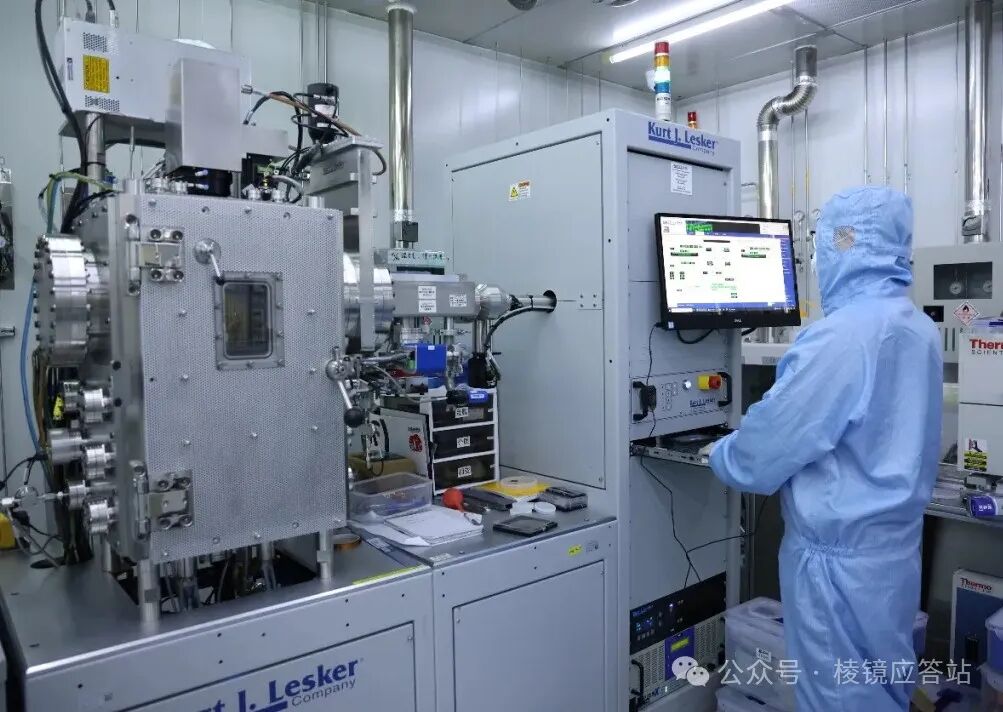
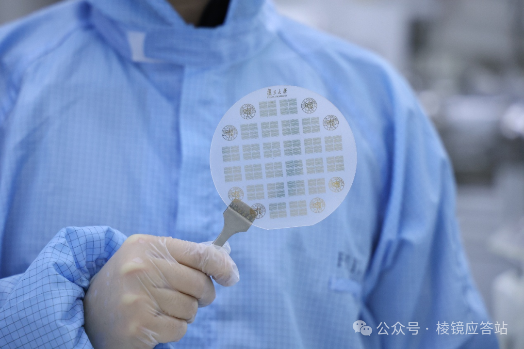
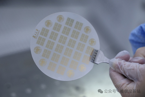
On a 12-inch wafer, a molybdenum disulfide film is evenly grown, with a thickness of only 0.7 nanometers, yet it bears the ultimate ambition of China’s semiconductor breakthrough. The Fudan team’s groundbreaking atomic-level interface control technology allows 5,900 transistors to achieve the power consumption levels of 28nm silicon-based chips under micron-level processes.
This strategy of “exchanging space for energy efficiency” is akin to a top-level Go master engaging in multi-dimensional games on a two-dimensional board—while traditional players are obsessed with the arms race of process miniaturization, Chinese researchers have opened a new battlefield in the material dimension.
The 99.77% yield data of the inverter reveals the core secret of this technological revolution. Through AI-driven one-stop collaborative process optimization, the team compressed the parameters of hundreds of processes from astronomical numbers to an operable range. This “algorithmic alchemy” approach has made the engineering challenges of two-dimensional semiconductors easily manageable.
As researcher Bao Wenzhong stated: “70% of our processes are compatible with existing silicon-based production lines, but the remaining 30% of core processes are all proprietary patents.” This clever, incremental innovation not only avoids the technological blockade of EUV lithography machines but also reserves a smooth transition interface for industrialization.
 The ecological ambition behind the power consumption revolution
The choice of the RISC-V architecture undoubtedly reveals the deep strategic considerations within China’s semiconductor industry. Under the patent walls built by ARM and x86 architectures, the ‘Wuji’ chip achieves “technological decolonization” at the architectural level through its open-source instruction set.
This ecological layout is less a technical choice than a projection of geopolitical dynamics in the microelectronics field—when 32-bit instructions execute smoothly on two-dimensional semiconductors, the competition for global chip standard-setting has quietly entered the second half.
Measured data shows that at a frequency of 1kHz, the computation power consumption is 0.43mW, indicating a significant breakthrough in the battery life of IoT devices. But this is merely the surface; the deeper transformation lies in the shift of computational paradigms.
Professor Zhou Peng’s declaration of “achieving nano-level power consumption with micron processes” essentially reconstructs the chip performance evaluation system. While the entire industry is obsessed with transistor density, China is redefining the technical discourse power based on energy efficiency.
This disruptive change in evaluation standards is akin to the replacement of physical keyboards by touch interactions in the smartphone era, both bringing about significant transformations.
 Reconstruction of power in the post-Moore era
The emergence of the ‘Wuji’ chip coincides with a critical juncture in the global semiconductor industry’s century-long upheaval. The massive investment in TSMC’s 3nm factory and Intel’s strategic shift back to foundry services seem clumsy in the face of the two-dimensional semiconductor revolution. Although this proof-of-concept chip has not yet reached commercial performance, the technological path it reveals is already shocking—when silicon-based processes approach physical limits, China’s choice of a “lane change overtaking” strategy is bringing the semiconductor race into a new dimension.
Industry impact assessments need to break out of traditional frameworks; two-dimensional semiconductors are not a replacement for silicon-based chips but a catalyst for reconstructing the industry landscape. Just as there is a symbiotic relationship between subways and buses, emerging materials will form a complementary ecosystem with mature technologies.
However, behind this technological equality lies a brutally harsh industry reshuffle—those giants who have invested hundreds of billions of dollars in silicon-based fields may face systemic risks of core patents devaluing in an instant.
This disruptive innovation’s dimensionality reduction strike is the strategic fulcrum for China’s semiconductor breakthrough. Standing at the critical point of technological revolution, the value of the ‘Wuji’ chip far exceeds the scope of laboratory results.
It marks a historic leap for China’s semiconductor industry from a state of following innovation to original innovation; it also signifies a profound restructuring of the global technological power structure.
As the atomic ripples of two-dimensional semiconductors spread throughout the industry, this seemingly silent revolution will ultimately stir up tremendous waves—China, mastering core technologies, is rewriting the new rules of the game.
(Note: This article is based on public information and reports for in-depth analysis, aiming to share knowledge and provide information.)
#WujiChip##FudanUniversityTeam##TwoDimensionalSemiconductors#