Skip to content
Perhaps some team is designing an embedded inference engine for edge computing, or is furthering automotive vision processing, or perhaps they possess insights in the data center domain that can challenge NVIDIA and Google! However, amidst the broad performance demands, environments, and applications, AI accelerator architectures face unique challenges not only in design but also in verification and implementation. Transitioning from an architecture to FPGA (which is almost a mandatory step in this field), and then to production ASIC, will be an extraordinary journey. However, for experienced and well-prepared design teams, with proper planning in advance, this may not necessarily mean a risky venture!
If, like most R&D teams, you choose to conduct proof of concept or validation on FPGA, you will be pulled in three directions from the very beginning, as shown in Figure 1. The architect team wants the FPGA implementation to be as close as possible to their microarchitecture because for them, the key is to see how effectively the design implements their algorithms. Meanwhile, the software team will push for performance design optimizations on the FPGA, which means making some compromises on the architecture to fit the capabilities and limitations of the selected FPGA chip. At this point, marketing pressure must also be considered, especially if they plan to leverage FPGA to enter the market early. In fact, there is a risk that the proof of concept itself will take on a life of its own, much like the creature of Frankenstein.
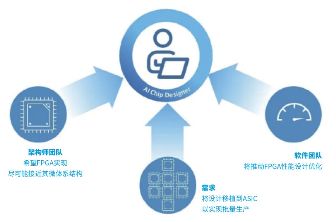 Figure 1: If you choose to conduct proof of concept or validation on FPGA, you will be pulled in the following three directions, coming from: the architect team, the software team, and manufacturing requirements.
If the first two steps of the design are architecture and FPGA design, the third step requires migrating the design to ASIC for mass production. This will bring the performance, power, and area needed for product competitiveness. Ideally, ASIC design will accurately reflect the original theoretical architecture, combined with optimizations for the selected ASIC process and IP library. However, even with the transfer of validated FPGA designs, the extent to which an excellent ASIC design can be achieved remains a crucial question. The answer will depend on the degree of collaboration between the architect team and the FPGA and ASIC teams.
The best way to support this statement may be to thoroughly study various architectural features of AI accelerators and follow them during the design process.
Parallel processing is the most common and fundamental aspect of AI accelerators. It can be achieved through many small dedicated processing cores (like GPUs for specific algorithms) or in a data flow manner (i.e., pipelining of dedicated processors). However, both of these architectures pose significant challenges for FPGA implementation.
The design team can encode processing units and their interconnections in RTL and hand over the RTL to FPGA design tools. However, to obtain a design with sufficient device resource utilization and performance, it typically requires nearly 100% routing, or at least manual intervention in floor planning and layout.
It is important to note that this planning will not focus on the prototype architecture of the accelerator but rather on the availability and location of resources in the FPGA. For example, the architecture may prefer to cluster computing units in local groups, whereas the FPGA may require distributing computing units across the chip or even splitting them into smaller blocks to ensure sufficient routing and RAM resources. This may necessitate changes to the interconnection architecture, such as altering the bus architecture.
However, other options may arise. For example, the architecture team for deep learning inference accelerators often utilizes lower precision algorithms (say, 8 bits instead of 32 bits) to increase speed and save energy. For performance and resource reasons, the FPGA team may wish to utilize the FPGA’s 32-bit multiply-accumulate hard macros instead of 8-bit multipliers built from logic units. Such choices will gradually move the FPGA design away from the original architecture and impact the conversion process.
At this point, it is time to transition the implementation to ASIC. In small, simple SoCs, the conversion from FPGA to ASIC means a nearly mechanical step-by-step conversion process. Remove any dedicated FPGA features, such as multiply-accumulate blocks, high-speed serial interfaces, PCIe interfaces, and DRAM controllers. Then replace them with functionally equivalent ASIC IP, and make any necessary changes to internal buses or interfaces to achieve efficient interconnections among them. Next, logic synthesis needs to be redone, and new clock networks and self-test architectures need to be inserted, power allocated, and verification performed.
This still holds true for AI accelerators. Any entity working in FPGA can be converted to ASIC in this way. However, what about the design changes made by the design team to optimize the FPGA design? The answer is that since the logic and routing resources in ASIC are essentially unlimited, and there is a large amount of third-party IP libraries, the changes made for FPGA will be unnecessary and may even have counterproductive effects.
The conversion team must understand the original design intent to decide whether to utilize the FPGA design or revert to the original architecture based on the specific circumstances. This is certainly true for determining which code to synthesize and how to best utilize IP.
Another example regarding memory may help in fully understanding this. Due to the parallel architecture of memory, AI accelerators typically utilize many small RAM instances of different shapes, sizes, types, and speeds within or between processing units. This practice fully aligns with the advantages of ASIC design but may severely disrupt FPGA. While a single FPGA logic unit group can be converted into small RAM within a logical architecture, design teams often utilize large, hard-wired, configurable RAM blocks in FPGA design. This leaves the FPGA team with two options: either modify the original architecture to use large shared RAM blocks instead of many smaller RAM blocks, or design a wrapper around the large RAM in FPGA to simulate a batch of smaller instances, hoping not to exhaust the routing resources near the RAM blocks.
Figure 2: The transition from FPGA to ASIC offers more choices. Specific decisions depend on the clarity of understanding of the design intent.
When transitioning from FPGA to ASIC, there are more choices, as shown in Figure 2. Should the conversion team directly convert the FPGA design (implementing the RAM block functionality of FPGA in ASIC design, which should not be difficult for experienced converters)? Or should the team revert to the original architecture with many dispersed RAM instances (where smaller RAM will be faster, more energy-efficient, and may restore the original architecture’s data flow, eliminating potential memory bottlenecks)? Ultimately, how to decide depends on the team’s understanding of the design intent.
Another issue is the multi-chip FPGA problem. Many accelerator designs are too large for a single FPGA and must be distributed across multiple chips. Thus, the communication method between these chips will impact the conversion process.
For example, if the FPGA is connected via a high-speed parallel bus (such as a memory bus), the design team can migrate everything from FPGA to ASIC and then connect them using the same parallel bus, like utilizing PCIe interfaces to connect multiple FPGAs. In this case, the design team will have to remove the PCI interfaces and replace them with direct parallel connections or possibly on-chip networks based on the nature of the data flow between blocks. It is also crucial to review the original architecture to see if any modifications were made to accommodate the insertion of inter-chip interfaces (e.g., by inserting large buffer memories or creating messaging protocols) and to exclude those changes.
Once the functional design is converted, work can proceed to the clock architecture. Here again, ASIC is not subject to many constraints imposed by FPGA. The conversion team can study the operational theory of the original architecture and fully leverage all opportunities it provides for local clock domains, gating, and frequency shifting, as all of these are easily accessible in ASIC.
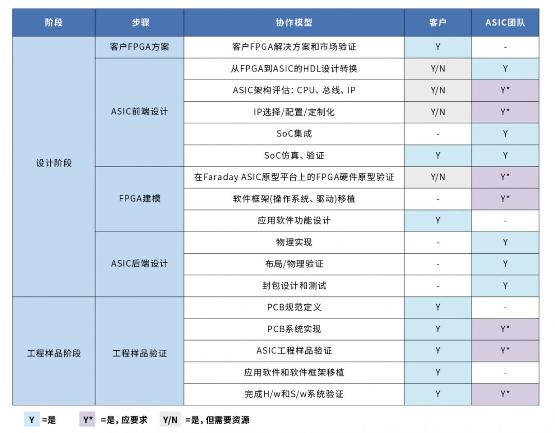
Figure 3: This table outlines each step in the FPGA to ASIC conversion process and clarifies implementation responsibilities.
Similarly, experienced conversion teams can utilize the parallel architecture of the accelerator to implement parallel built-in self-test, leveraging their clear understanding of design intent and thorough knowledge of testing provider capabilities. In fact, this optimization not only transcends ASIC design itself but also delves deeper into the supply chain. If all parties fully understand and implement the content and responsibilities of the steps shown in Figure 3, it will significantly reduce testing costs, thereby significantly saving overall unit costs.
At this point, it has been seen that converting AI accelerator design from intermediate FPGA to ASIC is almost a mechanical process. However, due to the highly parallel nature of AI and accelerators, for the conversion team, achieving better results is possible if they can fully understand the nuances of the original design intent and architecture, recognize FPGA-specific optimizations, possess AI semiconductor design experience, and can freely allocate tasks between customers and ASIC team experts.
However, it is always essential to remember that the ultimate goal is to achieve an ASIC with excellent power, performance, and area, which is the original design intent.
Figure 1: If you choose to conduct proof of concept or validation on FPGA, you will be pulled in the following three directions, coming from: the architect team, the software team, and manufacturing requirements.
If the first two steps of the design are architecture and FPGA design, the third step requires migrating the design to ASIC for mass production. This will bring the performance, power, and area needed for product competitiveness. Ideally, ASIC design will accurately reflect the original theoretical architecture, combined with optimizations for the selected ASIC process and IP library. However, even with the transfer of validated FPGA designs, the extent to which an excellent ASIC design can be achieved remains a crucial question. The answer will depend on the degree of collaboration between the architect team and the FPGA and ASIC teams.
The best way to support this statement may be to thoroughly study various architectural features of AI accelerators and follow them during the design process.
Parallel processing is the most common and fundamental aspect of AI accelerators. It can be achieved through many small dedicated processing cores (like GPUs for specific algorithms) or in a data flow manner (i.e., pipelining of dedicated processors). However, both of these architectures pose significant challenges for FPGA implementation.
The design team can encode processing units and their interconnections in RTL and hand over the RTL to FPGA design tools. However, to obtain a design with sufficient device resource utilization and performance, it typically requires nearly 100% routing, or at least manual intervention in floor planning and layout.
It is important to note that this planning will not focus on the prototype architecture of the accelerator but rather on the availability and location of resources in the FPGA. For example, the architecture may prefer to cluster computing units in local groups, whereas the FPGA may require distributing computing units across the chip or even splitting them into smaller blocks to ensure sufficient routing and RAM resources. This may necessitate changes to the interconnection architecture, such as altering the bus architecture.
However, other options may arise. For example, the architecture team for deep learning inference accelerators often utilizes lower precision algorithms (say, 8 bits instead of 32 bits) to increase speed and save energy. For performance and resource reasons, the FPGA team may wish to utilize the FPGA’s 32-bit multiply-accumulate hard macros instead of 8-bit multipliers built from logic units. Such choices will gradually move the FPGA design away from the original architecture and impact the conversion process.
At this point, it is time to transition the implementation to ASIC. In small, simple SoCs, the conversion from FPGA to ASIC means a nearly mechanical step-by-step conversion process. Remove any dedicated FPGA features, such as multiply-accumulate blocks, high-speed serial interfaces, PCIe interfaces, and DRAM controllers. Then replace them with functionally equivalent ASIC IP, and make any necessary changes to internal buses or interfaces to achieve efficient interconnections among them. Next, logic synthesis needs to be redone, and new clock networks and self-test architectures need to be inserted, power allocated, and verification performed.
This still holds true for AI accelerators. Any entity working in FPGA can be converted to ASIC in this way. However, what about the design changes made by the design team to optimize the FPGA design? The answer is that since the logic and routing resources in ASIC are essentially unlimited, and there is a large amount of third-party IP libraries, the changes made for FPGA will be unnecessary and may even have counterproductive effects.
The conversion team must understand the original design intent to decide whether to utilize the FPGA design or revert to the original architecture based on the specific circumstances. This is certainly true for determining which code to synthesize and how to best utilize IP.
Another example regarding memory may help in fully understanding this. Due to the parallel architecture of memory, AI accelerators typically utilize many small RAM instances of different shapes, sizes, types, and speeds within or between processing units. This practice fully aligns with the advantages of ASIC design but may severely disrupt FPGA. While a single FPGA logic unit group can be converted into small RAM within a logical architecture, design teams often utilize large, hard-wired, configurable RAM blocks in FPGA design. This leaves the FPGA team with two options: either modify the original architecture to use large shared RAM blocks instead of many smaller RAM blocks, or design a wrapper around the large RAM in FPGA to simulate a batch of smaller instances, hoping not to exhaust the routing resources near the RAM blocks.
Figure 2: The transition from FPGA to ASIC offers more choices. Specific decisions depend on the clarity of understanding of the design intent.
When transitioning from FPGA to ASIC, there are more choices, as shown in Figure 2. Should the conversion team directly convert the FPGA design (implementing the RAM block functionality of FPGA in ASIC design, which should not be difficult for experienced converters)? Or should the team revert to the original architecture with many dispersed RAM instances (where smaller RAM will be faster, more energy-efficient, and may restore the original architecture’s data flow, eliminating potential memory bottlenecks)? Ultimately, how to decide depends on the team’s understanding of the design intent.
Another issue is the multi-chip FPGA problem. Many accelerator designs are too large for a single FPGA and must be distributed across multiple chips. Thus, the communication method between these chips will impact the conversion process.
For example, if the FPGA is connected via a high-speed parallel bus (such as a memory bus), the design team can migrate everything from FPGA to ASIC and then connect them using the same parallel bus, like utilizing PCIe interfaces to connect multiple FPGAs. In this case, the design team will have to remove the PCI interfaces and replace them with direct parallel connections or possibly on-chip networks based on the nature of the data flow between blocks. It is also crucial to review the original architecture to see if any modifications were made to accommodate the insertion of inter-chip interfaces (e.g., by inserting large buffer memories or creating messaging protocols) and to exclude those changes.
Once the functional design is converted, work can proceed to the clock architecture. Here again, ASIC is not subject to many constraints imposed by FPGA. The conversion team can study the operational theory of the original architecture and fully leverage all opportunities it provides for local clock domains, gating, and frequency shifting, as all of these are easily accessible in ASIC.
Figure 3: This table outlines each step in the FPGA to ASIC conversion process and clarifies implementation responsibilities.
Similarly, experienced conversion teams can utilize the parallel architecture of the accelerator to implement parallel built-in self-test, leveraging their clear understanding of design intent and thorough knowledge of testing provider capabilities. In fact, this optimization not only transcends ASIC design itself but also delves deeper into the supply chain. If all parties fully understand and implement the content and responsibilities of the steps shown in Figure 3, it will significantly reduce testing costs, thereby significantly saving overall unit costs.
At this point, it has been seen that converting AI accelerator design from intermediate FPGA to ASIC is almost a mechanical process. However, due to the highly parallel nature of AI and accelerators, for the conversion team, achieving better results is possible if they can fully understand the nuances of the original design intent and architecture, recognize FPGA-specific optimizations, possess AI semiconductor design experience, and can freely allocate tasks between customers and ASIC team experts.
However, it is always essential to remember that the ultimate goal is to achieve an ASIC with excellent power, performance, and area, which is the original design intent.