The Field Programmable Gate Array (FPGA) is a key component in modern electronic systems, known for its highly flexible and powerful overall structure design. However, many beginners struggle to understand the overall structure of FPGAs. Let’s take a look at what components exist and their specific functions.
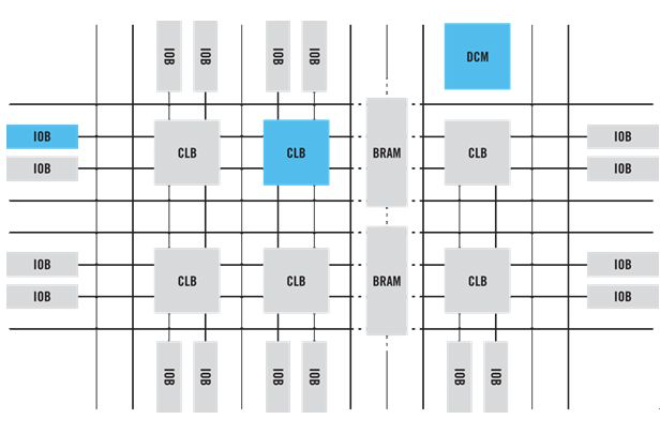
1. Configurable Logic Block (CLB)
Function: The CLB is the basic logic unit of the FPGA, responsible for executing most of the logical operations.
Structure: Each CLB contains a configurable switch matrix, which consists of 4 or 6 inputs, several selection circuits (such as multiplexers), and flip-flops.
Features: Once configured, the CLB can handle tasks such as combinational logic, shift registers, or RAM.
2. Input/Output Block (IOB)
The IOB is responsible for the interface between the FPGA and the external world, providing conversion of input and output signals.
Structure: The I/Os within the FPGA are grouped by banks, with each bank independently supporting different I/O standards.
Features: Supports multiple I/O standards, providing an ideal interface bridge for system design.
3. Internal Wiring
Function: Responsible for transmitting signals between CLBs and IOBs, achieving high-speed and flexible connections within the FPGA.
Structure: Wiring types include short line resources (for CLB interconnections), high-speed horizontal and vertical long lines (for device interconnections), and global low-skew wiring (for clocks and global signals).
Features: The complexity of the design is usually hidden by design software, so users do not need to focus on wiring details directly.
4. Other Embedded Units
Function: These units may include embedded RAM, DSP (Digital Signal Processing) blocks, high-speed serial transceivers, etc., to enhance the functionality and performance of the FPGA.
Structure: The types and quantities of embedded units vary based on the specific FPGA model and design requirements.
Features: Provide additional hardware acceleration capabilities, enabling the FPGA to handle more complex tasks.
This article is an original piece by Fan Yi Education. Please indicate the source when reprinting!