Source: Semi Connect
Author: Belle
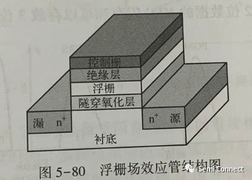
Flash Memory, also known as Flash, is a type of non-volatile memory that represents data using the threshold levels of storage cells. The main technology used in Flash memory cells is the Floating Gate field-effect transistor (see Figure 5-80). The charge on the floating gate determines the threshold of the field-effect transistor: programming increases the threshold by injecting electrons into the floating gate through the quantum tunneling effect, representing logic “0”; erasing does the opposite, removing electrons from the floating gate, decreasing the threshold, representing logic “1”.
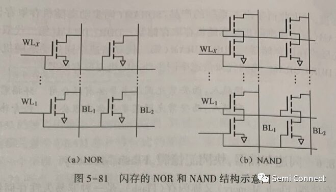
According to the different connection methods of storage cells, Flash memory is divided into NOR Flash and NAND Flash, as shown in Figure 5-81. NOR Flash cells are connected in parallel, which results in a larger area and smaller capacity compared to NAND Flash cells. The operation of NOR Flash is similar to SRAM and DRAM, allowing for fast random reads, making it suitable for code storage. NAND Flash cells are connected in series, forming a string of storage cells, which reduces the number of contact holes. The average area of a single NAND Flash storage cell is close to 4F² (F is the process feature size), offering higher integration than NOR Flash, with multiple storage cell strings forming storage cell blocks. The erase operation of NAND Flash is performed at the block level, while read and programming operations are conducted at the page level, making it ideal for large-capacity data storage applications. NAND Flash is commonly used in smartphones, digital cameras, MP3 players, and other electronic products; it can also be used to implement Solid State Drives (SSD) as a replacement for hard drives, providing advantages such as shock resistance, fast speed, noiseless operation, and low power consumption.
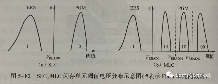
Based on the number of bits stored in a single storage cell, Flash is categorized into SLC, MLC, TLC, etc. The threshold voltage distribution of SLC and MLC Flash memory cells is illustrated in Figure 5-82. An SLC Flash cell stores 1 bit of information. To achieve higher storage density, multi-level (Muti-Level) Flash memory cells program the threshold voltage to multiple levels, allowing one field-effect transistor to store more than 1 bit of information. Currently, MLC Flash can store 2 bits per cell, and TLC Flash can store 3 bits per cell.
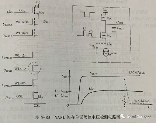
The number of bits that Flash memory cells can hold depends on the precision with which the threshold voltage can be programmed and detected. The threshold voltage of the storage cell is detected by adjusting the voltage on the selected word line. Different word line voltages will result in different discharge currents ICELL flowing through the storage cell, allowing the threshold voltage to be determined by recognizing the current magnitude. The threshold voltage detection circuit for NAND Flash memory cells is shown in Figure 5-83. First, node UOUT charges to UDD, and through the field-effect transistor MN, charges the bit line. Since the gate voltage of MN is U1, the bit line charges to voltage U1-UTHN, where UTHN is the threshold voltage. Then, MN is turned off, and node UOUT stops pre-charging. After the storage cell string is opened, the bit line begins to discharge, during which the voltage of the selected cell’s word line is UREAD. Finally, if UBL<U2-UTHN, then MN conducts and UOUT is pulled low, indicating that the storage cell’s threshold UT< UREAD; otherwise, MN is turned off, and UOUT remains high, indicating that the storage cell’s threshold UT>UREAD. The precision of the voltages U1, U2, and UREAD directly determines the precision of the threshold detection, requiring careful design of the related voltage generation circuits.
Retention Time is one of the important indicators of Flash reliability, indicating how long a Flash cell can retain data. In practical applications, due to defects in the insulating layer, the charge on the floating gate will gradually leak. Currently, manufacturers typically specify a retention time of 10 years. Endurance is a significant challenge in Flash design, as the gate oxide layer gradually deteriorates after multiple high-voltage operations, and with the reduction of process feature sizes, the coupling interference between adjacent floating gate cells becomes more severe. The number of times a cell can be erased and reprogrammed is limited. Currently, the typical endurance for SLC is 100,000 erase/program cycles, while MLC can be as low as 10,000 erase/program cycles or even lower. To address these challenges, one approach is to enhance the endurance of the storage cell itself through process improvements, such as charge trap Flash memory cells overcoming coupling interference between floating gate cells, allowing Flash technology to continue to shrink to the tens of nanometers; on the other hand, improvements in chip design can reduce the wear on storage cells during array operations, including adjusting the voltage values and duration of high-voltage operations, and introducing verification and programming prohibition mechanisms.

Editor: Liao Zhi