Source: The World of Photolithography
Storage is born alongside data; wherever there is data, there will be a need for storage chips. Moreover, with the development of emerging industries such as big data and the Internet of Things, the storage industry is closely related to information security. The total global output value of storage chips is about $80 billion, with the DRAM market at $45.7 billion, the NAND FLASH market at $30.6 billion, and the NOR FLASH market at $3.3 billion, indicating a vast market space for storage chips.
Storage is related to security, and the fundamental reason for strong policy promotion is the demand for self-controllability. In recent years, information storage security incidents have occurred frequently. Once information storage security is threatened, it will endanger the development of all industries, including government, military, petroleum, chemical, nuclear energy, finance, etc., making it a crucial part of national security strategy. Currently, China has a significant gap in storage chips, relying almost 100% on imports, which poses a severe information security situation. Therefore, China must vigorously promote the localization of storage chips.
Storage chips have four major characteristics: significant technological gaps, high industry concentration, strong cyclicality, and substantial capital investment, making the localization task arduous. A single domestic enterprise is unlikely to overcome these challenges, thus the national will is strongly promoting the localization of storage chips. Currently, Unisplendour has invested 60 billion yuan in a storage chip factory, with plans to invest $30 billion focusing on memory chip manufacturing; Wuhan Xinxin is investing $24 billion to build a memory base; Fujian Jin Hua Integrated Circuit is collaborating with UMC to develop niche DRAM with a 32-nanometer process, investing 37 billion yuan in storage chips; Hefei is investing 46 billion yuan to build a DRAM factory. We see that under the national will, multiple domestic forces have begun to promote the localization of storage chips. We also suggest that the Chinese government continually increase support for storage chips from multiple angles, including technical cooperation, talent support, system integration, and industrial chain support.
NAND FLASH has broad prospects, and 3D NAND FLASH is expected to achieve a leapfrog development in China. The replacement of HDDs with SSDs is a long-term trend, which can ignite the demand for NAND FLASH in the market. Currently, NAND FLASH is undergoing a comprehensive transformation from 2D to 3D, and transitioning from 2D to 3D requires new technological fields to join, leaving a breakthrough opportunity for Chinese manufacturers. If Chinese manufacturers can integrate cross-domain talent and technology, 3D NAND FLASH will become a critical entry point for China to leapfrog in storage chips.
DRAM market demand is steadily rising, and participation from Chinese manufacturers is expected to break the current pattern. Applications in mobile and enterprise sectors are further increasing the demand for DRAM. The overall demand for the DRAM market is showing a steady increase. Currently, the DRAM market is dominated by Samsung, SK Hynix, and Micron, but the continuous promotion of DRAM projects by Chinese manufacturers in the coming years is expected to disrupt the market pattern.
Investment recommendation: As a foundational chip in semiconductors, storage chips have significant strategic importance. We are optimistic about China’s efforts to develop the storage industry, which is expected to create a new camp. Relevant targets: 1) Storage chip industry leader: Unisplendour. 2) Packaging and supporting companies: Shenzhen Technology, Huatian Technology, Changdian Technology, Tongfu Microelectronics. 3) Material and equipment companies: Qixing Electronics, Shanghai Xinyang. Additionally, we are paying attention to Gigadevice (IPO approved).
Among these, we recommend Shenzhen Technology, as its subsidiary, Peidun Technology, has been supplying storage packaging and testing to Kingston and Micron for many years, with world-class technology and deep benefits from the localization of storage chips.
We primarily recommend Shenzhen Technology: Currently, Chinese manufacturers do not possess core technology for storage chips. As for the manufacturing side, partnerships with foreign entities are necessary, while domestic companies are most likely to deeply participate in the packaging and testing side. Peidun Technology has long supplied packaging and testing for Kingston and Micron, with world-class technology, and has been validated over time. As the country invests heavily in storage chips, the packaging and testing side will prioritize Peidun Technology as a supplier. Currently, the planned storage chip factories in China have a packaging and testing cost requirement exceeding 10 billion yuan, while Peidun Technology achieved revenue of 450 million yuan in 2015 (with a net profit of 137 million yuan, a profitable business), indicating significant potential. Shenzhen Technology’s traditional OEM business is gradually entering major clients such as Huawei and VIVO, with stable performance growth.
1. Wherever there is data, there is a need for storage!
(1) DRAM, NAND FLASH, and NOR FLASH are the three mainstream memory types.
Memory is one of the two core components of computer systems, alongside the central processing unit (CPU), digital signal processor (DSP), and programmable logic array (FPGA), and is a major strategic pillar product in the field of electronic information. As one of the four general-purpose chips, the significance of developing the storage chip industry is self-evident. For electronic products, it is as essential as food.
It is born alongside data; wherever there is data, there will be a need for storage chips. Moreover, with the development of emerging industries such as big data and the Internet of Things, the storage industry is closely related to information security.
Based on different storage media, storage chips can be divided into three major categories: RAM (random access memory), ROM (read-only memory), and solid-state drives; magnetic storage such as floppy disks, hard disks, and tapes; and optical storage like CDs and DVDs. Depending on the role of memory in computer systems, they can be categorized into main memory, auxiliary memory, cache memory, and control memory.
In 2014, the total output value of storage chips was approximately $80 billion, with the DRAM market at $45.7 billion, the NAND FLASH market at $30.6 billion, and the NOR FLASH market at $3.3 billion.
(2) The storage industry chain: IDM model dominates, manufacturing capability is crucial.
The industry chain of storage chips is similar to that of ordinary semiconductors, consisting of upstream chip design, midstream chip manufacturing, downstream chip packaging and testing, and ultimately the application of chips in end products. Unlike the vertical division of labor model of many semiconductor products (Fabless + Foundry + OSAT), storage chips predominantly adopt the IDM model, with the output value of the IDM model accounting for over 90% of the total output value of storage chips. In the international memory market, lessons learned from industry giants like Samsung, Micron, Toshiba, and Hynix, which transitioned from ‘survivors’ to ‘winners’, and the experience of Taiwanese memory manufacturers transitioning from ‘industry’ to ‘disaster’, show that memory is usually produced under the IDM model or a closely cooperative simulation IDM model. Pure memory foundry or detached memory design is unlikely to become the final winner.
The IDM model dominates the storage chip industry. This is due to the high standardization of storage chip technology, where the product capacity and packaging forms produced by different manufacturers adhere to standard interfaces, and performance differences are minimal. In a homogenous competitive environment, storage manufacturers can win the market by enhancing manufacturing processes, providing manufacturing capacity, and leveraging economies of scale to reduce costs. Thus, manufacturing capability is the core competency of storage manufacturers. As the complexity of storage chip manufacturing processes continues to rise, the investment required for manufacturing plants will increase significantly, demanding more stringent requirements for the financial strength and management capabilities of storage manufacturers. The vertical division of labor model (Fabless + Foundry + OSAT) can reduce investment risks for storage manufacturers, and its proportion is expected to rise. Currently, some storage manufacturers are forming joint ventures with packaging manufacturers or establishing similar IDM models through strategic cooperation to develop storage chips, effectively taking a step towards a vertical division of labor model.
2. The fundamental reason for strong policy promotion is the demand for self-controllability.
(1) Storage is related to security, and self-controllability is imperative.
1. Storage is the foundation of information security, and self-controllability is necessary to ensure security.
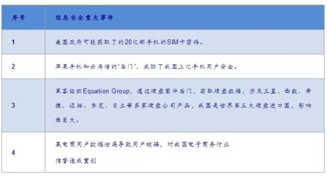
The higher the degree of social informatization, the more information data is generated, which makes the issue of information security more prominent. For many years, the focus of the information security industry has been on information transmission protection and attack defense, leading to the emergence of numerous network security devices such as firewalls, VPNs, IPS, and UTM, while neglecting the essential field of information storage security. Information storage security ensures the authenticity, confidentiality, integrity, availability, reliability, and non-repudiation of information throughout its lifecycle. Compared to information transmission security, a threat to information storage security can lead to the leakage of both current and past information, causing greater harm. This is crucial for the development of all industries, including government, military, petroleum, chemical, nuclear energy, finance, transportation, manufacturing, logistics, e-commerce, and water conservancy, making it an important part of China’s overall national security strategy. In the first quarter of 2015 alone, several information storage security incidents occurred, indicating a severe situation.
Table 1: Multiple information storage security incidents occurred in the first quarter of 2015.
To resolve China’s information storage security issues, it is crucial to achieve self-controllability of storage devices. All storage devices can be simplified into two parts: storage control chips and storage media. The storage medium is the most fundamental component, serving as the carrier of information, and its importance is self-evident. The storage control chip manages the input and output of information, serving as the ‘throat’ of information storage security. Ensuring the security of storage control chips effectively installs a ‘security door’ on the entire storage device. Most of the identified storage security incidents are related to backdoors in storage control chips, making self-controllability of storage control chips a key technology for information storage security products.
2. Storage chips rely on imports, and the demand for domestic alternatives is substantial.
China ranks first globally in the shipment of laptops and smartphones, with the rise of manufacturers like Huawei and Lenovo, as well as the explosion of data centers driven by internet companies like Alibaba, Tencent, and Baidu, resulting in a massive demand for storage from domestic manufacturers. In 2015, the estimated procurement scale of DRAM in mainland China was $12 billion, and that of NAND Flash was $6.67 billion, accounting for 21.6% and 29.1% of the global supply, respectively. These storage chips remain absent domestically, relying almost entirely on imports. As one of the key measures for national information security, once domestic manufacturers can produce high-performance storage chips, the government will guide numerous manufacturers to procure domestic storage chips, indicating a vast space for domestic alternatives.
(2) Four major characteristics of storage chips make localization tasks challenging, and the strength of a single domestic enterprise is insufficient to overcome these challenges.
1. Significant technological gaps.
The manufacturing process of storage chips is extremely complex, especially for 3D NAND flash, which is particularly challenging to manufacture. Currently, all global storage manufacturers keep their 3D NAND manufacturing processes highly confidential. Generally speaking, 3D NAND products are manufactured using a monolithic formation method, where after the first layer of NAND film is grown, photomasks and etching are used, followed by continuous growth and etching of 8 layers of film, culminating in the need for a single photomask, totaling 27 photomasks. This method was proposed by Toshiba in 2007. Currently, Samsung’s TACT, VSAT, Toshiba’s P-BiCS, and 3D VG all belong to the monolithic 3D memory technology.
Domestic manufacturing technology for NAND FLASH and DRAM is virtually non-existent. The Unisplendour Group has never been involved in the storage chip field, and merely relying on capital investment, without acquiring or collaborating with a strong memory manufacturer, makes it difficult to smoothly advance storage chip projects. The main technology of Wuhan Xinxin comes from cooperation with Spansion, and its 3D NAND stack may only have 8 layers, while the international mainstream stack is 32-48 layers, with Samsung’s technology reaching 64 layers, indicating a significant gap. Fujian Jin Hua Integrated Circuit’s DRAM technology is based on cooperation with UMC, while Hefei’s DRAM technology is based on collaboration with Zhaojin Technology, making it very challenging to acquire advanced core processes.
Additionally, intellectual property (IP) is a weapon in the chip industry competition. Currently, storage chip patents are almost monopolized by international giants. Whether it is Wuhan Xinxin or Fujian Jin Hua, their technology relies on technology licensing cooperation. If Chinese storage manufacturers achieve corresponding success in the coming years due to significant investments, an inevitable IP battle will follow.
2. High industry concentration.
The storage industry market concentration is high. Taking the DRAM market as an example, it started with about 40-50 companies in the 1970s, had 14 companies by the end of the 1990s, and only 5 prominent companies remained by 2004. Currently, only 3 companies dominate 90% of the market, resulting in a duopoly competition pattern among Samsung, SK Hynix, and Micron.
In such a monopolistic competitive environment, it is challenging for domestic manufacturers to emerge, especially in a storage industry that thrives on scale. Gaining a share of the global market from these giants is exceedingly difficult.
3. Strong cyclicality.
The high standardization of storage products means that manufacturing capability becomes the core competitiveness of storage manufacturers. Currently, the global memory industry maintains a balance of oligopoly among 4-5 major players, making coordination difficult. Under the surface, investment actions among these manufacturers are intense. If one company expands or reduces production, it will affect the global supply-demand situation for storage chips. When the industry is booming, they have sufficient funds to expand production capacity or upgrade processes. If any major storage manufacturer expands production, others will be pressured to do the same or risk losing market share, leading to a vicious cycle of excessive production and subsequent industry downturns. Conversely, during an industry downturn, major manufacturers begin to cut production, reversing supply-demand relationships, causing prices to rise and the industry outlook to improve.
Currently, major manufacturers such as Samsung, SK Hynix, Micron, Toshiba, and Sandisk are undergoing a new round of capacity expansion. We believe that after PCs and smartphones, there are currently no large-scale consumer products expected to emerge in the short term, and based on the cyclical characteristics of the storage industry, the balance state of the storage industry may be disrupted in the next 3-4 years.
4. Significant capital investment.
We refer to the capital expenditures of international storage chip giants. According to data from research firm Semiconductor Intelligence, in 2015, the capital expenditure budget for semiconductor companies was led by Samsung at $15.1 billion (excluding Samsung’s investments in other fields), a year-on-year increase of 13%; SK Hynix at $5.1 billion, a year-on-year increase of 12%; Micron at $3.8 billion, a year-on-year increase of 186%; and other storage manufacturers at $2 billion, a year-on-year increase of 43%. In 2015, the storage industry accounted for the highest proportion of overall semiconductor capital expenditure, reaching 38%.
Faced with these four major characteristics of storage, it is challenging for domestic manufacturers to achieve breakthroughs in storage chips without any technological advantages.
(3) Breaking through storage chips is underway, with national focus and direct engagement on the main battlefield.
Memory, like CPUs, is a strategic high ground in the chip field and a crown jewel of the chip industry, making it a primary battlefield rather than a guerrilla warfare situation.
Mainstream memory, whether DRAM or NAND, relies on advanced processes and scale. The United States, South Korea, and Japan have all followed this path. In the early 20th century, Taiwan accelerated investment in storage chips during the transition from 8-inch to 12-inch wafer factories, expecting to win by having the largest number of 12-inch wafer factories globally. However, this ultimately ended in failure. The failure of Taiwan in the memory field has multiple reasons, one of which is the Foundry model of Taiwanese storage chips, which relies on core technology from Europe and the United States, thus only producing inferior products and niche markets. Relying solely on scale to win is not feasible. Therefore, if China wants to develop the memory industry, it must grasp core technologies, recruit top talent, and acquire technology quickly; it must also prepare for long-term massive investments and potential losses. A cold bench may need to be endured for ten years before there is a chance to score a goal. Both aspects must not be neglected.
Grasping technology.
The semiconductor storage technology is developing rapidly, and in addition to related technologies, memory patents have also become competitive tools. According to iRunway statistics, the semiconductor memory industry has had significant patent layouts in traditional memory technologies (SRAM, ROM, DRAM, NAND FLASH) over the years. In the past 15 years, memory manufacturers have begun to focus on commercial layouts of alternative storage technologies such as FRAM, MRAM, PRAM, and RRAM. From the perspective of patent applicants, major manufacturers like Micron, Samsung, Toshiba, and Sandisk hold numerous core patents. Based on the application of foundational patents in the United States, Sandisk, Micron, and Intel possess the most foundational patents, with Micron, Samsung, Toshiba, IBM, and Intel holding about 25% of the total. Due to this monopoly on storage technology, patent litigation among memory manufacturers is common. Since 1993, the number of patents involved in semiconductor memory technology litigation has surged, with Sandisk, Conversant IP, TI, Rambus, and other companies involved in the most litigation.
In light of the current market situation of storage chip technology, Chinese manufacturers must adopt both external collaboration and independent research and development to master core storage technologies. In terms of external collaboration, traditional storage technologies (SRAM, ROM, DRAM, NAND FLASH) have become very mature, with key technologies controlled by Micron, Samsung, Toshiba, and Sandisk. Chinese manufacturers must target these companies for collaboration. For example, Unisplendour Group acquired 15% of Western Digital (which acquired SanDisk for $19 billion), Jiangbolong has strategic cooperation with Marvell, and Wuyuefeng Capital is involved in acquiring the American DRAM giant ISSI. In terms of independent research and development, emerging storage technologies such as FRAM, MRAM, PRAM, and RRAM are still in their infancy, and all companies are on the same starting line. Notably, according to the statistics from the National Intellectual Property Administration, as of October 30, 2014, there were 4,168 patent applications in the RRAM (resistive random-access memory) field globally, with applicants from the United States, Japan, and South Korea submitting the most patents, while Chinese applicants submitted 410 patents, ranking fourth. We believe that the key to developing new technologies lies in people, and Chinese manufacturers need to recruit experienced talents, such as Unisplendour Group’s plan to recruit Taiwan’s DRAM guru Gao Qiquan.
Competing on scale.
The design technology for storage chips is relatively simple, and the standardization of product forms is high, making it easy to expand market share. Storage chip manufacturers rely on mastering core technologies to compete on scale. South Korea, during the transition from 6-inch to 8-inch wafer factories, leveraged the capacity advantage of nine 8-inch wafer factories to replace Japanese manufacturers and ascend to the top of the global DRAM industry. Major storage manufacturers like Samsung, Micron, and Sandisk spend tens of billions or even hundreds of billions of dollars annually on capital expenditures to increase their market share through scale. For Chinese manufacturers to achieve breakthroughs in the storage industry, they must be prepared for long-term massive investments and potential losses, enduring a cold bench for a decade, similar to BOE’s development of LCD panels. Currently, Unisplendour Group is investing 80 billion yuan to build a storage factory, indicating plans to invest 300 billion yuan within the next five years to become the third largest chip manufacturer globally.
Whether grasping technology or scale, both are time-consuming and labor-intensive endeavors that require national strategic support to complete!
(4) As the battle for storage chips progresses, we recommend that the Chinese government continue to increase policy support.
1. Under national will, multiple domestic forces are already working to conquer storage chips.
Unisplendour Group: 60 billion yuan to build a storage chip factory, with plans to invest $30 billion in memory chip manufacturing over the next five years.
In 2015, Tongfang Guoxin raised 80 billion yuan through private placement, investing 60 billion yuan in a storage chip factory, acquiring 25% of Taiwan’s Powerchip for 3.79 billion yuan, and investing 16.2 billion yuan in acquisitions of upstream and downstream companies in the chip industry chain. For the new storage chip factory, once completed and fully operational, it is expected to add 120,000 pieces/month of storage chip production capacity. Additionally, the chairman of Unisplendour has stated plans to invest $30 billion in memory chip manufacturing in the future.
Wuhan Xinxin: $24 billion to build a memory base.
Wuhan Xinxin, established in 2006, previously operated a 12-inch wafer factory in cooperation with SMIC, but became independent in 2013 after SMIC exited the partnership. Wuhan Xinxin has focused on the development and production of memory products, primarily producing NOR Flash products until 2013, when it began developing 3D-NAND.
In March 2016, Wuhan Xinxin officially launched the memory base project, which will invest $24 billion (approximately 160 billion yuan) over five years, with funds primarily allocated to technology research and development, project infrastructure, equipment procurement, and industrial chain construction. If the funding and product development progress smoothly, the memory base is expected to start mass production in 2018, reaching a monthly production capacity of 300,000 pieces (with 200,000 pieces of 3D-NAND and 100,000 pieces of DRAM) by 2020, and 1 million pieces monthly by 2030.
This project is a crucial strategic initiative for Wuhan, with the province and city committing their resources to transform this memory base project into a billion-dollar high-tech industry project.
Fujian and Hefei: Fujian Jin Hua invests 37 billion yuan, Hefei collaborates with Zhaojin Technology to invest 46 billion yuan to build a DRAM factory.
Fujian: In May 2016, UMC announced a collaboration with Fujian Jin Hua Integrated Circuit to develop niche DRAM with a 32-nanometer process, with technology licensed to Jin Hua, which can also retain research outcomes. Fujian Quanzhou Jinjiang has planned 17,000 acres of land to construct an integrated circuit industrial park and successfully introduced the Fujian Jin Hua integrated circuit memory production line project, with a total investment of 37 billion yuan, included in the “13th Five-Year Plan” for major integrated circuit projects, becoming a national key supported DRAM production project.
Hefei: The Hefei municipal government has partnered with former Elpida president Sakamoto Yukio to establish Zhaojin Technology, introducing Japanese technology and investing 46 billion yuan to build a DRAM factory, expected to commence mass production in the second half of 2018, with a monthly capacity of 100,000 pieces of 12-inch wafers.
Recently, there are reports that Unisplendour Group is collaborating with Wuhan Xinxin to jointly tackle storage chips, further highlighting the national will to develop storage chips.
2. We recommend that the Chinese government increase support for the storage chip industry comprehensively, from talent to industrial chain support.
The localization of storage chips is a daunting task that requires tackling hard challenges. The four major characteristics of storage chips dictate that the localization project cannot be accomplished without strong support from the Chinese government. We believe that, in addition to financial support, the Chinese government should comprehensively and continuously increase support for the storage chip industry across various fields, including:
1) Technical cooperation. Major manufacturers like Micron, Samsung, Toshiba, and Sandisk hold core technologies for storage chips and have applied for numerous patents. The Chinese government should actively seek collaboration with manufacturers that possess core storage chip technologies to introduce and assimilate these technologies.
2) Talent support. The development of storage chip technology is fundamentally reliant on people. Chinese manufacturers need to recruit experienced talents, such as Unisplendour Group’s plan to recruit Taiwan’s DRAM guru Gao Qiquan. Additionally, Chinese manufacturers should focus on internal talent development, actively guiding university research resources toward industrialization.
3) Systematic integration to avoid resource waste. The Chinese government is advised to coordinate the overall development of storage chips, fully utilizing the advantages of domestic companies in the storage chip sector and mobilizing resources across departments to collectively tackle storage chip challenges.
4) Strengthening industrial chain support. The Chinese government should enhance industrial chain support, gradually nurturing domestic capabilities across all aspects of the supply chain, including design, manufacturing, equipment, and packaging/testing.
3. NAND FLASH: Broad prospects, 3D NAND FLASH is expected to achieve a leapfrog development in China.
(1) Mobile applications and SSDs are the two largest fields driving NAND FLASH demand.
FLASH memory is a non-volatile storage technology that allows for the erasure and reprogramming of memory cells organized into blocks, primarily including NAND and NOR flash technologies, each with distinct performance characteristics and applications. NAND FLASH’s primary advantage lies in its large storage capacity, making it suitable for high-capacity storage applications such as smartphones, tablets, enterprise SSDs, mobile storage, and USB drives. NOR FLASH, while having a smaller capacity, offers faster speeds and supports XiP, making it suitable for applications such as code storage in mobile phones, PC BIOS, DVDs, USB keys, set-top boxes, network devices, and IoT devices. Since NAND FLASH accounts for approximately 90% of the value of FLASH, we will focus on the development of NAND FLASH.
The two main application areas for NAND FLASH are mobile applications (smartphones and tablets) and SSDs. In mobile applications, to simplify storage usage, NAND Flash chips and control chips are designed as a single MCP chip, allowing downstream customers to procure eMMC chips without dealing with complex NAND Flash compatibility and management issues. In 2014, NAND FLASH accounted for 38% of smartphone applications and 10% of tablet applications. NAND FLASH’s share in SSD applications was 29%.
(2) The replacement of HDDs with SSDs is a long-term trend that can ignite NAND FLASH market demand.
1. SSDs outperform HDDs, and their replacement is a long-term trend.
Hard drives can be divided into mechanical hard drives (HDD) and solid-state drives (SSD). HDDs are traditional hard drives consisting of platters, read/write heads, spindle motors, and control electronics, while SSDs are made from arrays of solid-state electronic storage chips, primarily using FLASH chips for storage.
Compared to HDDs, SSDs have advantages such as faster data reading speeds, noiseless operation, strong resistance to shock and vibration, low power consumption, low heat generation, and a wide operating temperature range, making SSDs suitable for a wide range of applications, from consumer electronics to enterprise and industrial applications. They are applicable in various fields, including consumer electronics, enterprise management systems, industrial sectors, communications, aerospace, military, space exploration, video surveillance, internet monitoring, embedded devices, and energy sectors. Essentially, any field involving big data, high traffic, and significant business interactions can benefit from SSDs.
The replacement of HDDs by SSDs is currently hindered by price factors, but the long-term trend remains unchanged.
Despite the superior performance of SSDs, there is still debate in the market about whether SSDs will replace HDDs as the mainstream storage medium, with price being a focal point of contention. A typical 1TB mechanical hard drive costs about $50, or $0.048/GB, while a similarly positioned 64GB solid-state drive costs about $23, or $0.36/GB. This shows that the cost ratio of SSDs to HDDs is 15:1.
When considering data center-level comparisons, the differences are even more pronounced. We believe that HDDs have developed since the 1970s, and due to their mechanical architecture, hard drives cannot improve performance as semiconductors can through manufacturing process improvements. After more than half a century of development, the spindle speed of hard drives has not significantly increased, leaving little room for price reductions. In contrast, the price of SSDs is primarily determined by the cost of NAND FLASH. As a semiconductor product, continuous improvements in manufacturing processes, along with increasing user acceptance of SSDs, will lead to increased demand for NAND FLASH products, resulting in technical and scale effects that will drive rapid price declines. Over the past three years, the price of SSDs has dropped by half. As the price of SSDs continues to decline, their application range will also expand, making the long-term trend of replacing HDDs irreversible.
HDDs face challenges related to virtualization and random access, prompting the advancement of SSD solutions.
In recent years, data storage volumes have grown exponentially, fundamentally changing storage methods. This change is less related to the required storage volume and more to the intended use of storage. HDDs are cheap, readily available, and have large capacities, making them suitable for many storage scenarios, but they also have inherent limitations. During the data ‘read/write’ process, HDDs require physical movement of the read/write arm to achieve data read/write operations, making them adept at reading data stored sequentially within sectors and between sectors, minimizing the movement of the read/write arm. However, as operational characteristics and virtualization drive the development of random data storage, combined with the explosion of image and video data, this results in the read/write arm of traditional HDDs moving constantly, increasing system delays. With the growth of virtual machines and the volume of searchable data, these delays accumulate, leading to severe bottlenecks in HDD storage. This bottleneck is not due to a lack of storage capacity but rather a deficiency in data read/write speeds, causing significant system delays. For commercial users, these delays are not trivial; they could result in content providers losing numerous customers or trading companies missing out on billion-dollar trading opportunities.
Because SSDs have no moving parts, they eliminate this major disadvantage of HDDs. The physical characteristics of SSDs make them more suitable for random access data needs. In the previous discussion, we primarily focused on the cost of storage per gigabyte ($/GB). However, for commercial users, focusing solely on the cost per gigabyte is one-dimensional; they should consider the overall cost of achieving business outcomes. For example, using fewer SSDs to achieve the same results lowers capital expenditures; SSD systems require fewer hard drives, and their specifications are smaller, often allowing two SSDs to fit in the space of one HDD, leading to reduced operating expenses. Moreover, the average MTBF of SSDs is about 2 million hours, while that of HDDs is only 1.5 million hours, enhancing reliability. Therefore, even though the current cost per gigabyte of SSDs is higher, in certain specific business needs, the overall cost of SSDs can be more advantageous.
2. HDDs remain the mainstream storage medium, and the replacement by SSDs will ignite NAND FLASH market demand.
Despite the rapid decline in HDD shipments and the rise in SSD market share, HDDs still have a capacity advantage and will continue to be widely used in cold storage. Currently, global SSD shipments are about 80 to 100 million units, while global HDD shipments are about 600 million units, with SSDs accounting for approximately 15% of the total shipments. Considering that the average capacity of a single HDD far exceeds that of an SSD, the actual storage capacity of SSDs is much less than 15%. Therefore, the current storage market still belongs to HDDs.
HDDs have dominated the storage market for many years; from 1976 to 2014, HDD shipments have consistently increased, with a turning point occurring after 2010 when HDD shipments began to decline. WDC and Seagate, as representatives of HDD manufacturers, have seen their revenues decline since 2010, excluding the impact of the 2008 economic crisis. It was also around this time that SSDs began to emerge, gradually replacing traditional HDDs as a new force in the storage field.
NAND Flash is the core component of SSDs, accounting for 70-80% of the total cost of SSDs.
SSDs are primarily composed of storage chips (NAND Flash) and control chips (Controller). The storage chip NAND Flash serves as the data storage medium, occupying much of the SSD PCB board space and is the core component of SSDs. The capacity of SSDs is determined by NAND Flash, and its fast read/write speeds, low power consumption, and shock resistance are all based on the characteristics of NAND Flash.
The replacement of HDDs with SSDs will open up NAND FLASH market demand.
In 2015, the shipment capacity of NAND FLASH was approximately 80EB, with one-third used for SSDs, equating to a total capacity of 26EB for SSDs. In contrast, HDD shipments for that year were around 500EB. Considering that the cost per gigabyte of SSDs is higher than that of HDDs, the market scale (in terms of value) for SSDs still has significant room for growth. This does not even account for the explosive growth in demand from big data applications such as IoT and cloud computing. As previously discussed, HDDs face challenges related to virtualization and random access, while the random access data demands represented by IoT and cloud computing require SSDs as storage media. According to MTR’s forecast, the SSD market is expected to grow at a compound annual growth rate of 40.7%, increasing 15-fold to reach a scale of $229.5 billion by 2022. NAND FLASH, being a major component of SSDs, means that the rapid growth of SSDs will drive demand for NAND FLASH.
(3) Mobile storage configurations are diverse, with ‘capacity increase + price reduction’ driving continued growth in NAND FLASH demand.
1. Mobile devices have diverse storage configurations, and NAND FLASH determines the storage capacity of these devices.
The memory configuration of smartphones varies widely, consisting mainly of RAM and ROM. RAM is mainly LPDDR DRAM, which significantly impacts smartphone performance and is expensive, having evolved to LPDDR3. ROM refers to FLASH, which stores various data within smartphones, akin to a computer’s hard drive, directly related to the data storage capacity of smartphones. The combination of RAM and ROM is a critical consideration for smartphone manufacturers in selecting platforms. The mainstream configurations include MCP, eMCP, POP (Package on Package), and the separated approach of eMMC + LPDDR2, with the choice usually determined by the main chip platform and capacity dictated by market demand. MCP is a method of packaging NAND FLASH and LPDDR1 together, suitable for low-end phones. Currently, mainstream smartphones primarily use eMCP or the separated eMMC + LPDDR2 approach, where eMCP integrates NAND FLASH and the controller. We believe that regardless of the RAM and ROM combination method, NAND FLASH remains a crucial ROM carrier for smartphones, determining the storage capacity of mobile devices. The same applies to tablets.
2. Capacity increases and price reductions will continue to drive NAND FLASH demand in mobile devices.
The single-machine ROM capacity of mobile terminals continues to rise.
Initially, smartphone storage solutions used NAND MCP, with the minimum being 512M (NAND FLASH) + 265M (DRAM), and the maximum reaching 4G (NAND FLASH) + 4G (DRAM), with even larger configurations of 8G (NAND FLASH) + 8G (DRAM). Currently, the mainstream storage solutions for smartphones are 32G, 64G (NAND FLASH) + 2G, 3G (DRAM). For example, the maximum ROM capacity for Apple’s flagship phones has increased from 32G in the iPhone 4 to 128G in the iPhone 6, while Samsung’s maximum ROM has increased from 16G in the Galaxy S2 to 128G in the Galaxy S7, indicating that smartphone single-machine ROM capacities are continuously rising.
The decreasing price of eMMC will introduce more new terminal applications.
eMMC balances high-efficiency transmission with high-capacity storage, making it the mainstream storage solution for mobile devices (smartphones, tablets, smart boxes, wearable smart hardware, etc.). eMMC has historically been limited in its application in mid-to-low-end products due to the high prices of internal NAND FLASH chips. However, with the continual decline in eMMC prices, its applications will extend from smartphones to smart boxes, GPS terminals, mobile reading terminals, and other products, further broadening the application range of NAND FLASH.
(4) NAND FLASH is undergoing a new round of capacity expansion, and 3D NAND FLASH is expected to enable China to leapfrog ahead.
1. The transition from 2D to 3D NAND FLASH is comprehensive, making 3D NAND FLASH a trend.
In recent years, to meet the demands for small size and high capacity, NAND FLASH has been forced to develop toward high integration. Technologically, the 16 to 19 nanometer process has become the limit for NAND FLASH products, and any further attempts to shrink dimensions incur high costs and result in unstable storage bits. Meanwhile, 3D NAND can adopt higher processes in a planar layout, allowing particles to remain at 35 to 40 nanometers, increasing capacity through multi-layer structures, improving the yield per wafer, and lowering costs (the cost per unit capacity will be lower than current technologies) while maximizing the lifespan and reliability of flash memory.
As early as 2013, Samsung began mass production of 3D NAND FLASH. In 2014, Samsung released its first 3D NAND FLASH using a 2xnm process with 48 layers, significantly improving manufacturing cost-effectiveness and establishing itself as a leader in 3D NAND FLASH. Subsequently, other major manufacturers, including Toshiba, SanDisk, SK Hynix, Intel, and Micron, followed suit, planning to begin mass production in 2015.
2. The era of 3D NAND FLASH presents opportunities for Chinese manufacturers to leapfrog ahead.
As Flash enters the 2x nanometer process, the cost advantages brought by process miniaturization are becoming less significant, delaying the technological progress of international Flash manufacturers. Consequently, 3D NAND Flash has emerged as an important method for further cost reduction. The transition from 2D to 3D requires new technological fields to join, allowing traditional storage chip manufacturers to focus more on 3D packaging, providing Chinese manufacturers with additional time to make breakthroughs. If Chinese manufacturers can integrate cross-domain talent and technology, this will be an opportune moment for China to leapfrog in the storage chip sector.
From Wuhan Xinxin’s layout, we can also observe China’s engagement in 3D NAND FLASH. In May 2015, Wuhan Xinxin signed a cooperation agreement with Spansion to develop 3D NAND Flash technology and tackle challenges in this area.
4. DRAM: Market demand is steadily rising, and participation from Chinese manufacturers is expected to break the current pattern.
(1) Demand for mobile and enterprise applications will further increase, with overall demand steadily rising.
DRAM, invented in 1966 and commercially used since 1970, has matured by 1990 and is now an indispensable component for products such as PCs, smartphones, tablets, and servers. DRAM is typically supplied to the market in module form, with the most common being memory sticks for PCs. According to statistics, in 2014, PCs (using DDR memory for PCs) accounted for 31%, mobile phones (using low-power LPDDR) accounted for 32%, servers accounted for 12%, consumer electronics accounted for 4%, and other applications accounted for 21%. Although PC shipments have been declining in recent years, the shipment growth of smartphones has slowed, the per-device DRAM usage continues to increase, and the significant construction of global data centers will consume more enterprise-grade DRAM. Micron’s CEO Mark Durcan predicts that the application structure of the DRAM downstream market will change in the coming years, with mobile and enterprise markets gaining a larger share.
2. New markets have yet to open, and short-term DRAM demand is steadily rising.
Historically, the DRAM industry has experienced significant revenue fluctuations due to competitive expansions, but in recent years, benefiting from the ongoing popularity of global smartphones and relatively cautious expansion by manufacturers, the DRAM industry has entered a phase of stable growth over the past three years.
From recent quarterly industry developments, according to DRAMeXchange observations, the global DRAM total output value in the third quarter of 2015 was $11.298 billion, a slight decline of 1.2% from the previous quarter. However, the proportion of mobile memory in total revenue surged from 33.7% in the second quarter to 40% in the third quarter. As smartphone shipments continue to grow in the fourth quarter, the share of mobile memory in the overall DRAM market is expected to rise accordingly. However, due to excess supply in the market, the average selling price of DRAM continues to decline, and the off-season is approaching again, coupled with the increase in bit output due to 20/21nm enhancements, exacerbating the oversupply situation, making further price declines inevitable. Currently, manufacturers are strategically shifting the production capacity of standard memory, which has experienced the largest price declines, to server memory and mobile memory with higher profit margins and more stable prices, while bit output continues to grow, preventing a significant reduction in overall DRAM revenue scale.
The rapid growth of smartphones has boosted the DRAM industry’s performance in recent years. Although the per-device DRAM capacity will continue to rise, in light of the slowing growth of smartphones, declining PC shipments, and continued downward pressure on DRAM prices, along with the fact that emerging markets such as IoT, smart TVs, and wearable devices have yet to open up, we believe that short-term market demand for DRAM will remain steady.
(2) Participation from Chinese manufacturers is expected to break the DRAM pattern.
DRAM originated in the 1970s, and under the drive of scale effects, the industry has seen continuous consolidation, leading to a mature market today. On one hand, the industry started with 40-50 companies, reduced to 14 by the late 1990s, and only 5 prominent companies remained by 2004. Currently, three companies dominate 90% of the market, resulting in a duopoly competition pattern among Samsung, SK Hynix, and Micron. On the other hand, DRAM investment has become fatigued, with the average investment in DRAM worldwide being 42.1% of sales from 2004 to 2008, dropping to 21.5% from 2009 to 2013, and expected to decrease further to 15-20% by 2017. The reduction in investments for establishing new production lines and improving process levels, alongside enhanced monopolization and reduced competition, has paradoxically led to a 40% increase in average DRAM prices, resulting in a 28% increase in the overall DRAM market. Currently, establishing a new wafer production line costs about $5 billion, making it difficult for any new entrants to cross the threshold, aside from the three giants.
Under the national will, Unisplendour Group is recruiting Taiwan’s ‘DRAM guru’ Gao Qiquan to develop DRAM; Wuhan Xinxin is investing $24 billion (approximately 160 billion yuan) to develop storage chips, planning to achieve a monthly production capacity of 100,000 pieces of DRAM by 2020; Fujian Jin Hua Integrated Circuit is collaborating with UMC to invest 37 billion yuan in a DRAM production project; Hefei is partnering with Zhaojin Technology to invest 46 billion yuan in building a DRAM factory. With the construction of DRAM factories, Chinese manufacturers are expected to break the current DRAM pattern.
5. Investment strategy: Primarily recommend Shenzhen Technology.
We know that globally renowned memory manufacturers adopt the IDM model, which has been proven to be the best operating model for memory manufacturers through historical experience. However, we believe that, based on China’s national conditions, the Chinese memory industry will adopt a ‘virtual IDM’ model. What is the ‘virtual IDM’ model? It is a production and operation model characterized by government intervention, where manufacturing and packaging/testing are participated in by different manufacturers, potentially with shareholding relationships and mutual cooperation, rather than being entirely market-driven.
In this virtual IDM model, we believe that the manufacturing sector needs to consolidate national strength, and faster results can be achieved through industrial cooperation or acquisitions; the packaging and testing sector is relatively easier, with existing domestic manufacturers benefiting the most; while the localization of materials and equipment is a long-term trend, but there are significant short-term challenges.
Shenzhen Technology: Acquiring Peidun Technology to occupy the high ground of storage packaging and testing.
In 2015, the company acquired 100% equity of Peidun Technology (Shenzhen) Co., Ltd. for $110 million, extending its reach into the storage chip packaging and testing field. Peidun Technology primarily engages in the packaging and testing of DRAM and FLASH chips and has been invested in by American Kingston for many years, with its storage packaging and testing operations being world-class. Currently, Peidun Technology’s DRAM testing capacity is the largest in mainland China, and its module production capacity is also one of the largest memory module production bases globally, serving as Kingston’s largest distributor in Asia.
Peidun Technology offers one-stop services for memory/flash storage devices, completing the process from wafer to module assembly in less than 10 days. In terms of capacity, Peidun Technology’s DRAM testing capacity is the highest in mainland China, and its FLASH packaging capacity reaches tens of millions of units annually. We believe that after the acquisition by Shenzhen Technology, Peidun’s capacity will further increase. In terms of revenue, Peidun Technology achieved 450 million yuan in revenue in 2015, with a net profit of 137 million yuan.
Looking ahead at the competitive landscape of domestic storage chips, Peidun Technology is one of the few mainland companies that possess core capabilities in storage chip packaging and testing while achieving technological self-controllability. Under the national determination to develop storage chips, Peidun Technology is expected to become a bridgehead in conquering domestic storage chip packaging and testing.
Unisplendour: The vanguard of national storage initiatives.
Unisplendour Group is undoubtedly the core force in mainland China’s storage chip industry. In 2015, Tongfang Guoxin raised 60 billion yuan to invest in a storage chip factory (manufacturing sector) and 3.79 billion yuan to acquire 25% of Taiwan’s Powerchip (packaging/testing sector). In the next five years, they plan to invest $30 billion in the storage chip industry.
Gigadevice: Leader in NOR Flash.
Beijing Gigadevice is the largest locally designed serial NOR Flash enterprise in mainland China. In 2012, Gigadevice ranked fourth in the NOR Flash market in China, with sales of 830 million yuan, accounting for 11.1% of the market, trailing only behind Micron, Spansion, and Winbond. According to Chipright Consulting data, Gigadevice held 6% of the global NOR Flash market share in 2014, ranking fifth globally.
Gigadevice has developed rapidly in recent years. In 2008, the company successfully developed mainland China’s first 8M SPI NOR Flash chip, filling a domestic gap. In 2009, the company was the first to achieve mass production of SPI NOR Flash chips. By 2010, all chip capacities from 512K to 32M were in mass production. In 2011, the company achieved mass production of 64M to 128M capacity chips, advancing its process technology to 90nm. By 2012, the technology level was upgraded to 65nm. By the end of 2014, the company had cumulatively shipped over 2.8 billion storage products.

Official Account ID: imecas_wx


Long press to identify the QR code to follow us