

All users are familiar with the term “memory” because all electronic products require memory, and usually more than one type of memory is used. However, many people easily confuse the types, specifications, and forms of memory. For example, NAND Flash, DRAM often mentioned in industry news, as well as SRAM, SDRAM, DDR3, DDR4, NOR Flash… So, what are these?
Let’s start with a segment from Baidu Encyclopedia:Memory is a component used to store programs and data. For computers, having memory enables memory functions and ensures normal operation. There are many types of memory, which can be divided into primary memory and secondary memory based on their usage. Primary memory is also known as internal memory (referred to as RAM, while in Hong Kong and Taiwan it is called memory). Secondary memory refers to storage devices other than computer memory and CPU cache, which can generally retain data even after power is turned off. Common secondary storage devices include hard drives, floppy disks, optical disks, USB drives, etc.In simple terms, DRAM is the memory we commonly use, while NAND Flash is essentially doing the job of a hard drive.
(This section is a popular science explanation for computer novices, feel free to skip it.)Friends unfamiliar with PC knowledge often ask when purchasing devices, what is the difference between a hard drive and memory? My hard drive capacity is clearly 1TB, but why does my PC still run slowly?The difference between hard drives and memory lies in whether the data stored will remain after the power is turned off. Even when the power is off, the data on the hard drive does not disappear.However, when we need to process data, if the CPU has to directly fetch data from the hard drive, it will take too long. Therefore, “memory” acts as an intermediary bridge, first copying a portion from the hard drive into memory, allowing the CPU to directly access data in memory for processing. This is about several million times faster than directly fetching data from the hard drive.By opening the task manager, you can see the memory space occupied by currently running programs. Many people complain that Chrome consumes a lot of processing resources, and the memory usage is higher than other browsers, quickly exhausting memory when multiple tabs are open.So simply put, a computer operates like an office, drinking beverages, reading books, listening to music… The more things you want to use at once, the larger the desktop (memory) needs to be. But other things that are not needed at the moment will be stored in the drawer (hard drive). Therefore, no matter how large the hard drive is, if you want to execute many tasks at once, you still need to consider the size of the memory.Memory processes data faster than hard drives, but data disappears after power loss, and it is also more expensive than hard drives.Of course, there are more details in the hierarchy of memory. See the following text.In simple terms, there is also a storage space inside the CPU called Register. When processing, the CPU loads data from memory into the Register, then performs calculations on the numbers stored in the Register, and finally stores the results back into memory. After all, the CPU and memory are still two different chips, and directly fetching data from the same chip is faster.Another concept is Cache, which is the intermediary bridge between the CPU and memory.In terms of speed: CPU’s Register > Cache > Memory > Hard Drive. The higher the level (the closer to the CPU), the faster the speed, the higher the price, and the lower the capacity.
Classification of Memory
Electrical memory refers to memory that is electrically written and read, mainly divided into two categories, as shown in Figure 1:Volatile Memory (VM): Data exists when the power is on, and data is immediately lost when the power is off (data evaporates), such as SRAM, DRAM, SDRAM, DDR-SDRAM, etc.Non-Volatile Memory (NVM): Data exists when the power is on, and data can still be retained when the power is off, such as ROM, PROM, EPROM, EEPROM, Flash ROM, FRAM, MRAM, RRAM, PCRAM, etc.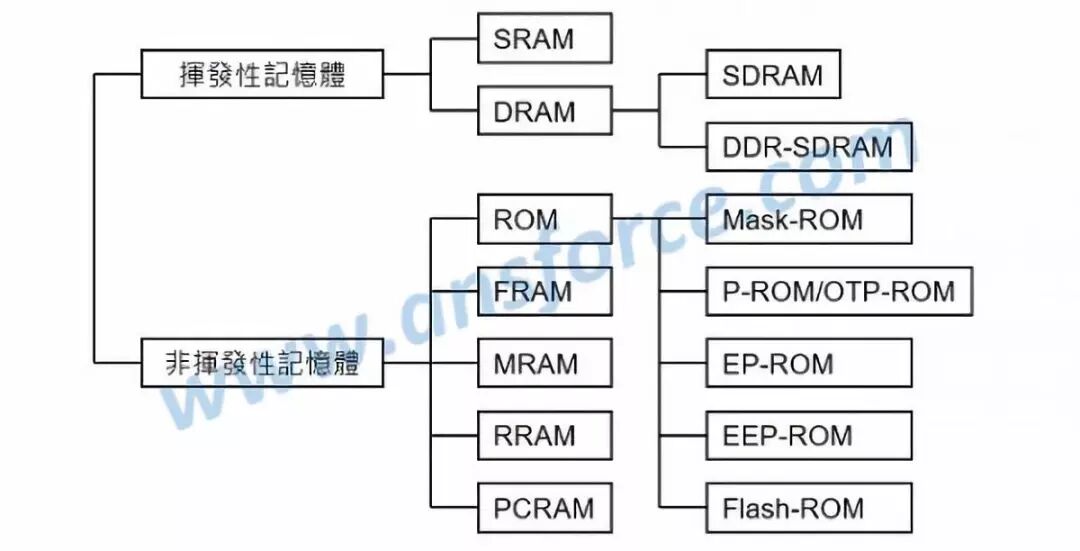 ▲ Figure 1: Classification of Memory.
Memory Cells
A memory “cell” refers to the smallest structure used to access data. If it contains one transistor (Transistor) and one capacitor (Capacitor), it is called “1T1C”; if it contains one transistor (Transistor) and one resistor (Resistor), it is called “1T1R”; if it contains one diode (Diode) and one resistor (Resistor), it is called “1D1R”.Each “cell” of memory does not necessarily store only 1 bit of data. As our demand for memory capacity increases, each “cell” can store more data, classified by the number of bits each “cell” can store: Single-Level Cell (SLC), Multi-Level Cell (MLC), Triple-Level Cell (TLC), Quad-Level Cell (QLC), etc.
Memory Hierarchy
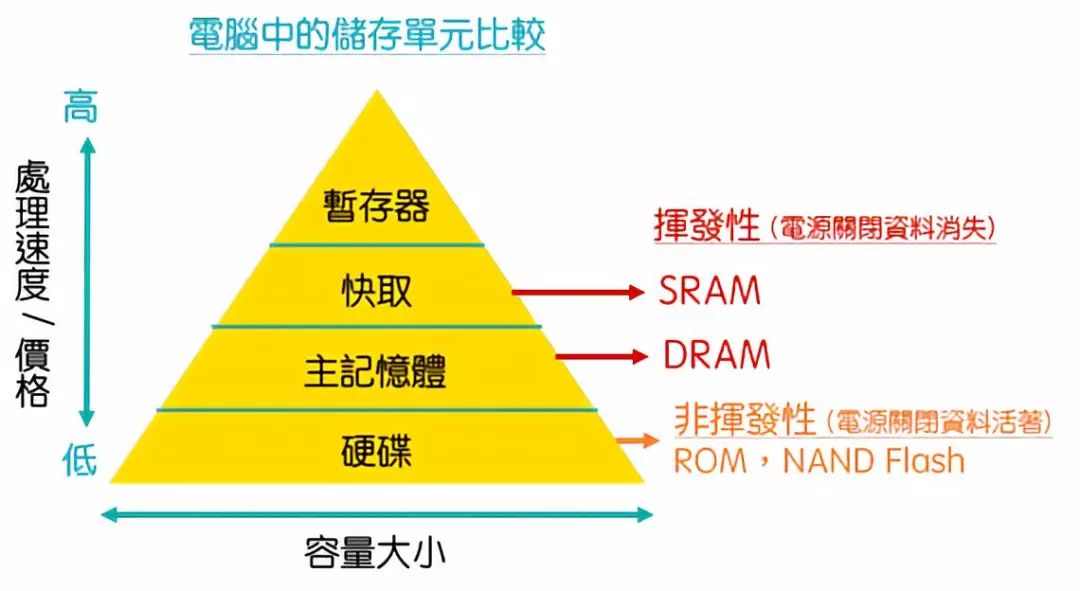
To understand the various memory configurations in electronic products, it is essential to introduce the concept of “memory hierarchy”. Memory hierarchy refers to how to properly allocate various types of memory with different storage capacities, processing speeds, and unit prices to achieve maximum economic benefits, ensuring reasonable processing speed, storage capacity, and product pricing.Figure 2 is a schematic diagram of the memory hierarchy, listed from top to bottom: Registers, Cache Memory, Main Memory, Secondary Memory:Registers: Inside the processor, used to set the functions of the processor, mainly a place to “temporarily store” setting values.Cache Memory: Inside the processor, used to “temporarily store” programs and data while executing programs, usually made with SRAM.Main Memory: Outside the processor, used to “temporarily store” programs and data, usually made with DRAM, which has now been improved to SDRAM or DDR.Secondary Memory: Outside the processor, used to “permanently store” programs and data, including flash memory, disk drives, optical drives, tape drives, etc.Different types of memory have different storage capacities, working speeds, and unit prices:Storage Capacity: Secondary Memory (GB) > Main Memory (MB) > Cache Memory (KB) > Registers (B).Working Speed: Secondary Memory (1ms) < Main Memory (10ns) < Cache Memory (1ns) < Registers (1ns).Unit Price: Secondary Memory < Main Memory < Cache Memory < Registers. ▲ Figure 2: Schematic Diagram of Memory Hierarchy.
Applications of Memory
All electronic products must use memory, and usually more than one type of memory is used. Due to the variety of memory types, users often get confused. We will briefly explain the differences between different memories. Figure 3 shows the system block diagram of the main chips in a mobile phone, including: Application Processor, Baseband Processor, Motion Controller.The Application Processor mainly executes the Operating System (OS) and Application Programs (Apps). Registers and Cache Memory are currently built into the processor, where Registers are used to set the functions of the processor, and the program that sets the Register values, which is used to drive hardware, is also called “Firmware”. Cache Memory is used to “temporarily store” programs and data while executing programs. Since it is closer to the processing unit within the processor, it can shorten the time for programs and data to travel back and forth, thus speeding up program execution, hence it is called “Cache”.Due to the high cost of Cache Memory, its capacity is limited. If it cannot fit while executing a program, it can fall back to Main Memory. However, the SDRAM or DDR used in Main Memory is a type of volatile memory, meaning that data is immediately lost when the power is turned off. Therefore, after shutting down, data must be stored in non-volatile Secondary Memory. Early Secondary Memory used disk drives, optical drives, tape drives, etc. Due to advancements in semiconductor processes, most now use flash memory (Flash ROM), or what is known as Solid State Drives (SSD), which are also made from flash memory.Since Cache Memory (SRAM) and Main Memory (SDRAM, DDR) are used to “temporarily store” programs and data for program execution, they are directly connected to the processing unit via a bus, and are generally calculated in “bits” for capacity; while Secondary Memory is used to “permanently store” programs and data, and since one byte can store one half-width character, it is generally calculated in “bytes” for capacity.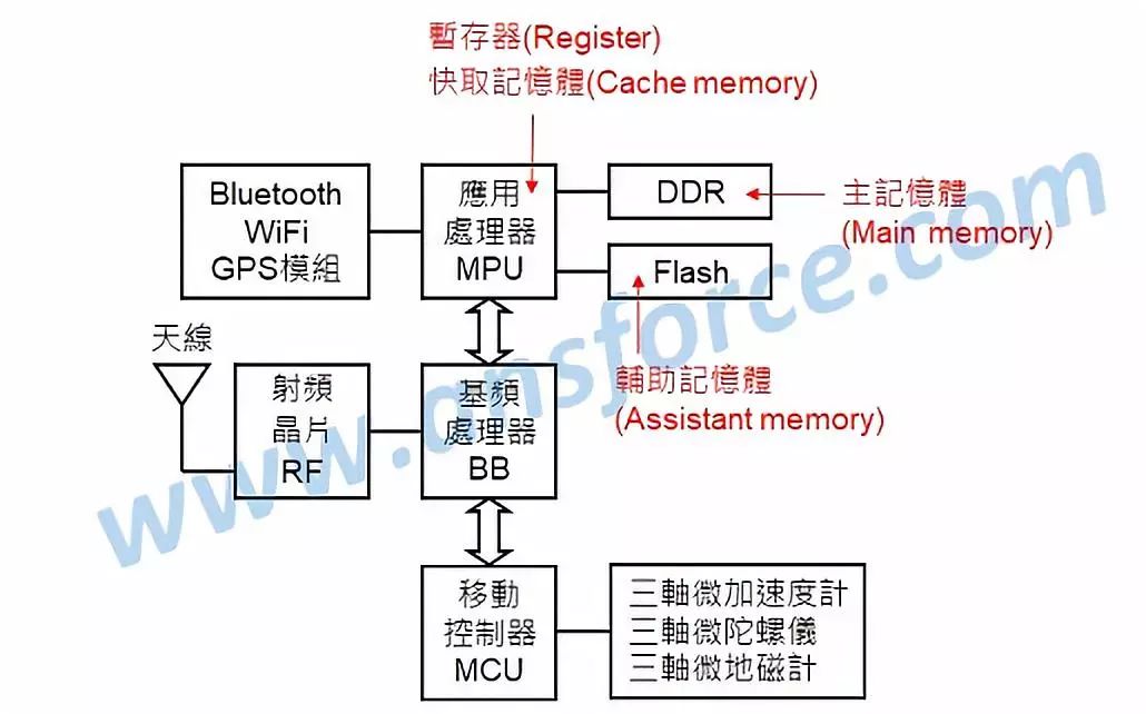 ▲ Figure 3: System Block Diagram of Main Chips in a Mobile Phone.Static Random Access Memory (SRAM)Stores 1 bit of data using 6 transistors (MOS), and does not require periodic power replenishment to maintain the memory content, hence it is called “Static”.SRAM has a more complex structure (6 transistors store 1 bit of data), does not use capacitors, so the access speed is faster, but the cost is also higher. Therefore, it is generally made into memory with lower capacity requirements but higher speed requirements, such as Cache Memory (Cache) built into CPUs, typically 256KB, 512KB, or 1MB.Dynamic Random Access Memory (DRAM)Stores 1 bit of data using one transistor (MOS) and one capacitor (Capacitor), and requires periodic power replenishment to maintain the memory content, hence it is called “Dynamic”.DRAM has a simpler structure (one transistor plus one capacitor), but the charging and discharging of the capacitor takes longer, resulting in slower access speeds, but it is also cheaper. Therefore, it is generally made into memory with higher capacity requirements but lower speed requirements, such as DDR-SDRAM used in personal computer motherboards, typically over 1GB. As processor speeds have increased, traditional DRAM speeds can no longer meet requirements, so it has now been improved to SDRAM or DDR-SDRAM.Synchronous Dynamic Random Access Memory (SDRAM)When the CPU accesses data from the main memory (SDRAM) on the motherboard, the “clock” (Clock) is the same, hence it is called “Synchronous”. Since the CPU does not need to “wait” when accessing data, the efficiency is higher. SDRAM access speeds are faster than DRAM, so early computer motherboards used SDRAM to replace traditional DRAM, but currently, only a few industrial computers still use SDRAM.A simple conclusion to remember: SRAM is faster, DRAM is slower; SRAM is more expensive, DRAM is cheaper.
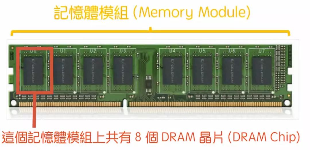 This is the memory we commonly use in computers, more accurately referred to as a “memory module”. A memory module is actually composed of a small circuit board and several DRAM chips. The memory module in the diagram contains a total of 8 DRAM chips. Let’s take a look at the internal structure of a DRAM chip, where we will see a storage array (Memory Array).The CPU will provide “row addresses” and “column addresses” to this storage array to select a “storage cell”. Common storage cells contain 4 bits or 8 bits, with each bit using a circuit structure, which we refer to as a “basic storage unit” of DRAM.This basic storage unit contains one transistor matched with one capacitor. Then, we can determine the current memory state by whether the capacitor has a charge or not.
 The action of “writing to memory” is performed by external data lines charging or discharging the capacitor, thus completing the writing of the digital data 1 or 0.DRAM uses one transistor (MOS) and one capacitor to store one bit of data (either a 0 or a 1). As shown in Figure 4 (a), when the transistor (MOS) is off, there is no electron flow, and the capacitor has no charge, indicating that this bit of data is 0. As shown in Figure 4 (b), when the transistor (MOS) is on (positive voltage is applied to the gate), electrons flow from the source to the drain, and the capacitor has a charge, indicating that this bit of data is 1. To “store” these incoming charges, a small capacitor must be used, as shown in Figure 4 (c). DRAM is slower than SRAM because the capacitor requires time to charge.▲ Figure 4: Structure and Working Principle of Dynamic Random Access Memory (DRAM).Due to the phenomenon of capacitor leakage, which leads to insufficient potential difference and causes memory loss, unless the capacitor is periodically charged, data cannot be ensured to be stored for long periods.Since the circuit structure of each basic storage unit of DRAM is very simple, it has low power consumption and is also cheaper. This allows for the production of large-capacity DRAM chips at low cost. The downside is that the read and write speeds are slow (due to the capacitor needing to charge and discharge), which affects the performance of DRAM.SRAM has a more complex structure, consisting of six transistors. We can label them as M1, M2, M3 to M6. These six transistors together can store one bit.
 SRAM chips are different from DRAM chips; they do not need to be divided into row addresses and column addresses for selection, and the design of SRAM is relatively more flexible. The number of storage units corresponding to one address can be 8 bits, 10 bits, or even 32 bits, 40 bits, or 64 bits.Additionally, the switching speed of transistors is much faster than the charging and discharging speed of capacitors, so the read and write speeds of SRAM are much faster than those of DRAM.However, to store one bit in SRAM, six transistors are required. As the number of transistors increases, the chip area becomes larger, making it difficult for integrated circuits to become smaller and leading to higher prices.(The price of SRAM is over 1000 times that of DRAM. For example, in 2010, the price per unit of SRAM was $60/MB, while DRAM was $0.06/MB.)At the same time, each transistor consumes power, and the more transistors there are, the higher the power consumption. Considering the high price and power consumption, SRAM can currently only be used in very demanding situations, such as the aforementioned Cache.Therefore, the current “main memory” still uses DRAM technology, but small portions used to speed up are Cache, which uses SRAM. However, whether DRAM or SRAM, data will be lost if power is not supplied, so both are called volatile memory.Ferroelectric Random Access Memory (FRAM)Dynamic Random Access Memory (DRAM) stores one bit of data using one transistor and one capacitor. Since traditional DRAM capacitors use “silicon oxide” as the insulator, and the dielectric constant of silicon oxide is not large enough (K value is not high enough), it is not easy to attract (store) electrons and holes, resulting in the need to constantly replenish electrons and holes, hence it is called “dynamic”. Once the computer’s power is turned off, the electrons and holes stored in the capacitor will be lost, and the data stored in DRAM will also be lost.To solve this problem, the simplest solution is to use materials with a high dielectric constant (high K value) to replace “silicon oxide” as the insulator, allowing electrons and holes to be stored in the capacitor without loss. Currently, the industry uses “lead zirconate titanate” (PZT) or “bismuth tantalate” (SBT), which are ferroelectric materials with a high dielectric constant (high K value), to replace silicon oxide, thus transforming the originally “volatile” dynamic random access memory (DRAM) into a “non-volatile” memory called “ferroelectric random access memory” (FRAM).
What about NAND Flash?
Continuing with the non-volatile part:Flash memory, due to its advantages of being lightweight, compact, and low power consumption, is used in various electronic products as hard drives. Flash can be divided into NOR Flash and NAND Flash.NOR Flash was introduced to the market earlier than NAND Flash. It has a faster read speed but slower write speed and is also more expensive than NAND Flash.Currently, it is used to store operating system program codes or important data, such as being used as ROM. For example, the Taiwanese manufacturer Winbond, which produces NOR Flash, has seen its revenue rise this year due to entering the ROM supply chain for the Nintendo Switch.NAND Flash has a fast write speed and lower price, making it the most common type. Today’s USB drives and mobile phone storage primarily use NAND Flash as the mainstream technology.Additionally, Solid State Drives (SSD) are also storage devices built on NAND Flash. SSDs do not have motors, read/write arms, and other components like traditional hard drives (HDD). They are slow, consume high power, and are sensitive to vibrations, making them difficult to use in small mobile devices.SSDs operate silently when reading and writing data, are shock-resistant, have fast transfer speeds, and can reduce weight to less than one-tenth of HDDs. They have now become the mainstream storage devices for personal computers and laptops.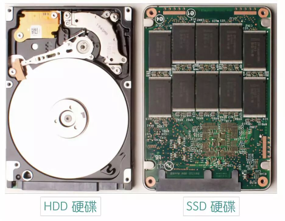 Summary:
-
Based on whether data can be retained after power is turned off, memory is divided into “volatile” and “non-volatile” storage.
-
Volatile storage is divided into DRAM and SRAM.
-
SRAM is faster but more expensive, so main memory often uses DRAM, while Cache often uses SRAM.
-
Non-volatile storage is divided into ROM and Flash, mainly used as hard drives.
-
Flash is further divided into NOR Flash and NAND Flash, with most hard drives now being based on NAND Flash SSDs.
 ▲ Q: Which memory manufacturers, such as DRAM, SRAM, Flash, represent which layer?Author: Li XiaoyaoSource: Technology Makes Dreams Greater