1. Case Background
The sample sent for inspection is a certain type of PCBA board. After SMT, it was found that some pins on a connector had poor soldering and unstable failure. Each side of the connector has a total of 50 pins, made of copper with nickel and tin plating. The PCB pad surface uses OSP technology, and the solder paste composition is Sn-Ag-Cu (95%-3%-0.5%).
2. Brief Description of Analysis Method
2.1 Visual Inspection of Samples
By observing the failed samples and normal samples under a stereo microscope, it was found that some pins of the failed samples indeed exhibited poor soldering. The positions of the failed pins were distributed irregularly on the connector, but the failures were mainly concentrated in the middle area of the connector, while the pins at both ends had relatively good soldering. Typical photos are shown in Figure 1. The normal sample showed full soldering at both ends, while the middle area had insufficient soldering, as seen in Figure 2. This phenomenon indicates that the failure may be related to position.
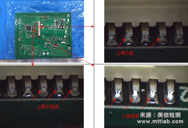
Figure 1 Typical Magnified Image of Failed Sample
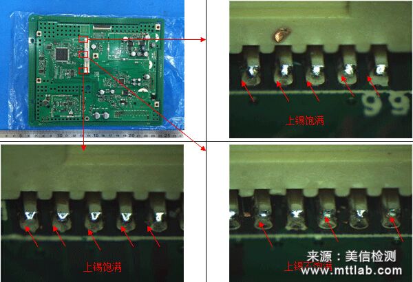
Figure 2 Typical Magnified Image of Normal Sample
2.2 Surface Analysis
As shown in Figures 3-4, surface SEM observation and EDS composition analysis were performed on the NG solder joints and unused pin surfaces. The composition test results are shown in Tables 1-2, with no significant contaminating elements found, indicating that the poor soldering of these pins is not significantly related to contamination.
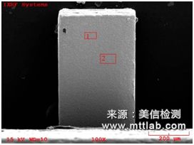
Figure 3 SEM Image and EDS Spectrum of NG Solder Joint Surface
Table 1 EDS Test Results of NG Solder Joint Surface (Wt%)
|
Spectrum |
C |
O |
Ni |
Cu |
Sn |
Total |
|
Position 1 |
3.34 |
4.83 |
/ |
1.15 |
90.68 |
100.00 |
|
Position 2 |
2.83 |
4.58 |
/ |
/ |
92.59 |
100.00 |
|
Position 3 |
2.99 |
5.51 |
0.82 |
/ |
Sn |
100.00 |
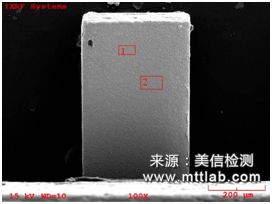
Figure 4 SEM Image and EDS Spectrum of Unused Pin Surface
Table 2 EDS Test Results of Unused Connector Pin Surface (Wt%)
|
Spectrum |
C |
O |
Sn |
Total |
|
Position 1 |
2.75 |
5.27 |
91.98 |
100.00 |
|
Position 2 |
2.74 |
5.43 |
91.82 |
100.00 |
2.3 Cross-Sectional Analysis
NG solder joints were sliced transversely and longitudinally to observe the internal connection of the solder joints:
As shown in Figure 5 and Table 3, longitudinal slicing shows that a good IMC layer forms between the solder and the pad, while separation occurs between the pin and the solder, with foreign substances present in the layering. The composition analysis of the foreign substances reveals that the main elements are C, O, Sn, and Br, which may be suspected as flux;
As shown in Figure 6 and Table 4, transverse slicing reveals that the NG solder joint pins are misaligned with the pad, showing that the solder does not wet the sides, while solder and pad form a uniform and continuous IMC layer. There is also layering between the pin bottom and the solder, with foreign substances present in the middle. Upon magnified observation of the layering, it is found that a layer of tin exists at the bottom of the pin, which is composed of pure tin (as shown in positions 1 and 2 in Figure 6); while the solder composition contains a small amount of Ag (positions 4 and 5), corresponding to the solder paste composition (Sn-Ag-Cu: 95%-3%-0.5%). Thus, it can be inferred that the tin layer at the bottom of the NG solder joint pin is the tin plating layer on the pin surface, indicating that during the SMT reflow process, the bottom of the pin did not have good contact with the solder.
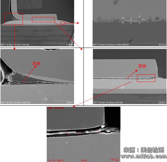
Figure 5 SEM Image and EDS Spectrum of Longitudinal Slice of NG Solder Joint
Table 3 EDS Test Results of Foreign Substances Between the Bottom of NG Solder Joint Pin and Solder (Wt%)
|
Spectrum |
C |
O |
Br |
Sn |
Total |
|
Position 2 |
31.35 |
8.10 |
23.08 |
37.48 |
100.00 |
|
Position 3 |
26.99 |
5.78 |
25.18 |
42.05 |
100.00 |
|
Position 4 |
28.60 |
4.33 |
18.51 |
48.55 |
100.00 |
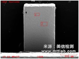
Figure 6 SEM Image and EDS Spectrum of Transverse Slice of NG Solder Joint
Table 4 EDS Test Results of NG-3# Solder Joint Pin Bottom and Solder (Wt%)
|
Spectrum |
C |
O |
Cu |
Ag |
Sn |
Total |
|
Position 1 |
1.06 |
0.78 |
0.70 |
/ |
97.46 |
100.00 |
|
Position 2 |
1.07 |
0.77 |
0.57 |
/ |
97.59 |
100.00 |
|
Position 3 |
13.51 |
16.40 |
1.75 |
/ |
68.35 |
100.00 |
|
Position 4 |
1.19 |
0.89 |
1.15 |
3.52 |
93.26 |
100.00 |
|
Position 5 |
1.23 |
0.92 |
0.93 |
2.30 |
94.63 |
100.00 |
2.4 Component Analysis of Pin Delamination
The NG solder joints were mechanically delaminated, revealing that the delamination force of the pins was small, indicating that the connector pins were poorly soldered. After separation, many foreign substances were found on the solder surface and the bottom of the pins. FTIR composition analysis of the foreign substances detected mainly carboxylic acid structures, indicating that these foreign substances were indeed flux, as shown in Figures 7-9. The significant residual flux suggests potential issues with furnace temperature, such as insufficient preheating time or low peak temperature. Surface observation of the PCB end solder joints and pins after delamination showed that the solder on the pad wetted well and had a shiny, smooth surface, further confirming that during the reflow process, the pins did not contact the solder.
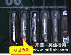
Figure 7 Image of Solder After Delamination
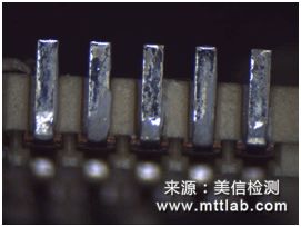
Figure 8 Image of Pins After Delamination
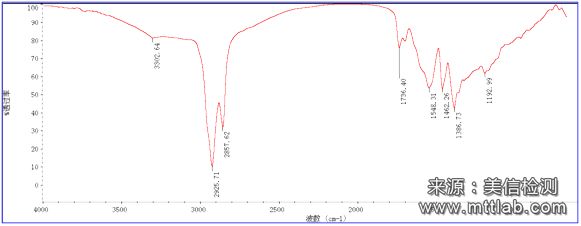
Figure 9 FTIR Spectrum of Foreign Substances on NG Solder Joint Surface
2.5 Solderability Analysis
To verify the correlation between poor soldering of the pins and their solderability, the standard IPC-J-STD-002C-2008 was referenced for solderability testing of component leads, terminals, solder pads, and wires. A solderability simulation test was conducted to confirm the solderability of the unused connector pins.
Three unused connectors were randomly selected, and flux was evenly applied to the pins, which were then immersed in a lead-free tin-titanium furnace at 255°C for testing. After maintaining for 5 seconds, the samples were removed and observed under a stereo microscope. The surface of the unused connector pins was found to have a continuous solder coating, meeting the standard requirements of IPC-J-STD-002C, as detailed in Figure 10. The results indicate that the solderability of this batch of connector pins is good, ruling out the possibility of poor solderability causing the pins to have poor soldering.
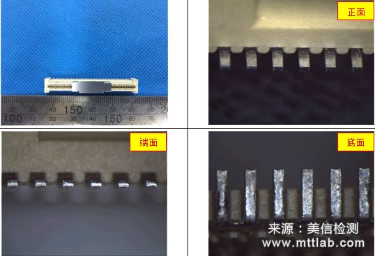
Figure 10 Image of Solderability of Unused Connector Pins
2.6 Analysis of Pin Flatness During Reflow
To determine the deformation of the component during the reflow process, the SMT furnace temperature curve was used to monitor the degree of deformation of the pins in real-time. The pin numbers are shown in Figure 11, and the results are in the appendix. The flatness curve is shown in Figure 12. From the test results, it can be seen that before soldering, the flatness of the connector pins was good. During the reflow process (220°C and peak temperature), some pins in the middle of individual connectors showed significant deformation (see connector 1), indicating that during the reflow process, some pins of individual connectors may undergo significant deformation, adversely affecting soldering.
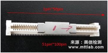
Figure 11 Schematic Diagram of Pin Numbers
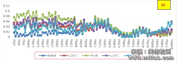
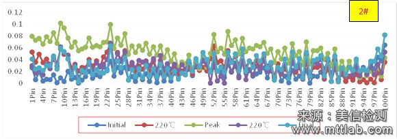
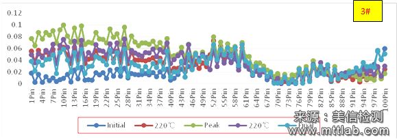
Figure 12 Curve of Pin Flatness at Various Temperatures
2.7 Verification Analysis of Furnace Temperature
Due to the significant residual flux on the surface of the NG solder joint, to confirm the impact of the furnace temperature curve on solder quality, real-time monitoring of the temperature of the connector pin solder joints was conducted:
Using the furnace temperature curve and chain speed provided by the customer (950mm/min), the temperature of the solder joints on the connector and other components was measured, with the test positions shown in Figure 13. The test results are shown in Figure 14. The peak temperature of the connector solder joint (position 2) during reflow was 234°C, while the peak temperature of the component solder joint (position 1) was 242°C. It can be seen that the connector pins absorbed a large amount of heat during the reflow process, resulting in a lower peak temperature, which adversely affects the wetting ability.
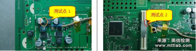
Figure 13 Schematic Diagram of Furnace Temperature Testing Positions
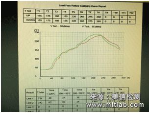
Figure 14 Furnace Temperature Test Curve
3. Analysis and Discussion
Based on the analysis results above, the reasons for the poor soldering of the connector pins can be summarized as follows:
Through the above testing and analysis, it can be concluded that the poor soldering is not significantly related to external contamination; through cross-sectional analysis and post-delamination analysis, it is found that the NG solder joints are poorly soldered, with internal layering between the pins and solder, and a large amount of residual flux present in the layering. The solder is smoothly distributed on the pad, indicating that during the reflow process, the pins did not contact the solder. The main reasons for solder joint layering are threefold: ① poor solderability of connector pins; ② co-planarity issues of connector pins; ③ improper furnace temperature settings.
Through solderability verification analysis, the issue of poor solderability of the connector pins can be ruled out; based on the deformation measurement results of the pins during the reflow process, it is found that the connector meets the co-planarity requirement of less than 0.1mm at room temperature, but individual connector pins in the middle may experience significant thermal deformation at 220°C or peak temperature, exceeding the printed solder paste thickness of 0.12mm, resulting in poor contact between the pins and solder during the reflow process; verification of the furnace temperature shows that the measured peak temperature of the connector pins is lower than that of other component pins by 8°C, which adversely affects the wetting ability and solderability of the pins.
4. Conclusion
The main manifestation of poor soldering on the connector is the lack of contact between the bottom surface of the pins and the solder joints. The reasons for this failure are twofold: ① thermal deformation during the reflow process; ② low temperature of the connector pins during the reflow process, affecting wetting performance.
5. Recommendations
1. Increase the solder paste thickness in the middle area of the connector appropriately;
2. Optimize the soldering furnace temperature curve and chain speed (priority direction).
6. Reference Standards
1. GJB 548B-2005 Microelectronic Device Testing Methods and Procedures Method 5003 Failure Analysis Procedures for Microcircuits
2. IPC-J-STD-002C-2008 Solderability Testing of Component Leads, Terminals, Solder Pads, and Wires
About Meixin:
Shenzhen Meixin Testing Technology Co., Ltd. (MTT) is a commercial laboratory with CNAS and CMA accreditation, focusing on providing customers with material and component testing, analysis, and technical consulting services. The service objects involve electronic and electrical, automotive, aerospace, new energy, new materials, education, and research industries. The company successfully went public on the New Third Board in December 2015, stock code: 835052.
Meixin Testing was established in 2012 and has set up multiple testing and analysis laboratories in Shenzhen and Suzhou, including microanalysis, surface analysis, chemical analysis, thermal analysis, electrical performance analysis, non-destructive structural analysis, physical performance testing, and reliability verification. By leveraging scientific testing and analysis standards or methods, professional engineering technicians, and precision instruments and equipment, we help customers solve various engineering, scientific, and technical problems related to materials and components encountered in product development, production, and trade.
Meixin Testing is committed to becoming a leader in the material testing, analysis, and technical consulting industry.



1、【Member Style】Shenzhen Zhixin Group has been deeply engaged in intellectual property for 8 years
2、【Collection Image】In June 1985, China’s first high-end Chinese microcomputer, the Great Wall 0520-CH, was born in Beijing
3、【Shenzhen Association Dynamic】Mr. Bai Xiaoyu, General Manager of Huaxia Happiness Industry Development Group, visited our association
4、【Industry Dynamics】The 2020 China Chip Application Innovation Design Competition officially launched, and members are welcome to actively sign up for the competition