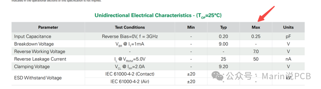
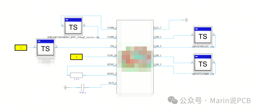
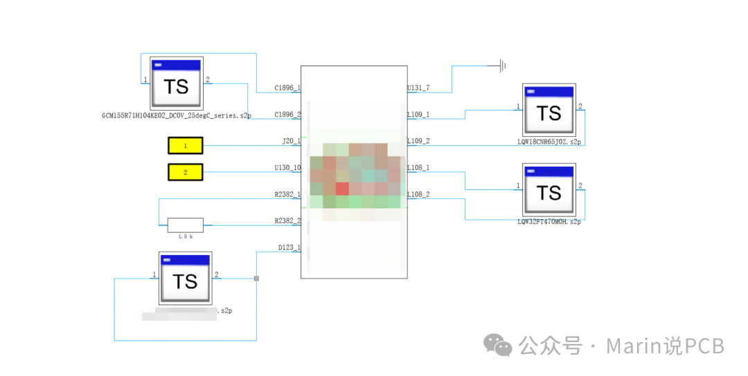
1. By comparing six CASE simulations of the schematic diagram to find the situation that best matches the actual test results:
A: Only the parasitic parameter model of ESD is imported (the S-parameter model of the FAKAR interface is not imported). Note: Only the parasitic capacitance values of ESD are added, not the actual S-parameters of the device.
 Editor
B: Only the S-parameter model of the FAKAR interface is imported (the parasitic parameters and S-parameter data model of the ESD device are not imported).
C: The S-parameter models of both devices are not imported (this approach was taken under ideal simulation conditions, and there is a deviation from the actual measurement). Note: The S-parameter model of the FAKAR interface is not imported, treated as an ideal 50-ohm impedance PORT.
D: Only the S-parameter data model of the FAKAR interface is imported, and the ESD is imported as a parasitic parameter data model. Note: The FAKAR interface imports the actual S-parameter model of the device, while the ESD device only imports its own parasitic parameters, not the actual S-parameters of the device.
E: The S-parameter models of both devices are imported (the worst-case simulation scenario, which somewhat matches the actual measurement). Note: The FAKAR interface imports the actual S-parameter model of the device, and the ESD device also imports the actual S-parameter data model.
F: Only the S-parameter model data of the ESD device is imported, and the S-parameter model of the FAKAR interface is not imported, treated as an ideal 50-ohm impedance PORT.
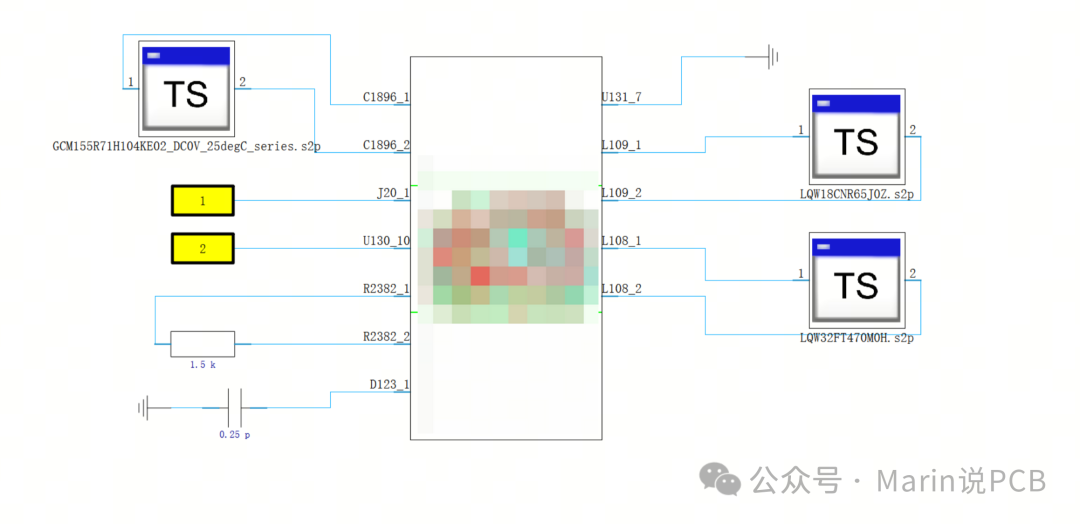
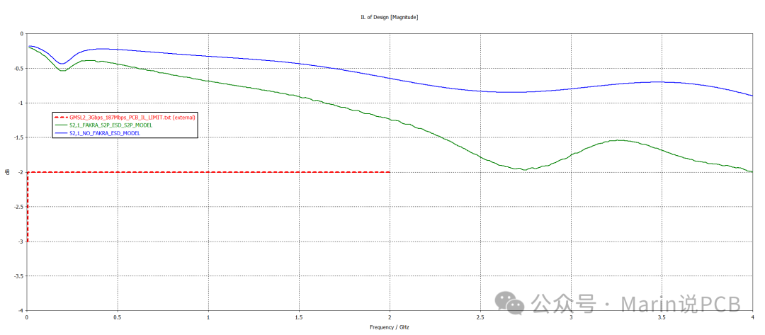
1. In the RX1_96724F_FAKRA_3 network, only the parasitic parameter model of ESD is imported, and the S-parameter model of the FAKAR interface is not imported, treated as an ideal 50-ohm impedance PORT. Let’s look at its simulation results:
 Editor
IL:
 Editor
RL :
 Editor
2. In the RX1_96724F_FAKRA_3 network, only the S-parameter model of the FAKAR interface is imported (the parasitic parameters and S-parameter data model of the ESD device are not imported). Let’s look at its simulation results:
 Editor
IL:
 Editor
RL :
 Editor
3. In the RX1_96724F_FAKRA_3 network, neither the ESD nor the FAKAR interface S-parameter models are imported (a relatively ideal simulation environment, without considering the impact of parasitic parameters from the FAKAR interface and ESD device). Let’s look at its simulation results:
 Editor
IL:
 Editor
RL :
 Editor
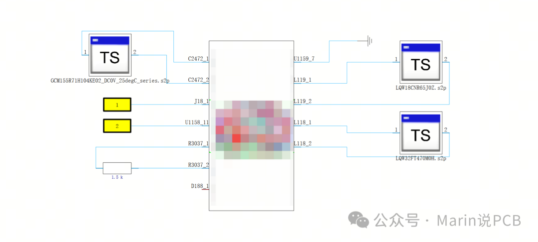
4. In the RX1_96724F_FAKRA_3 network, only the S-parameter data model of the FAKAR interface is imported, and the ESD is imported as a parasitic parameter data model. Note: The FAKAR interface imports the actual S-parameter model of the device, while the ESD device only imports its own parasitic parameters, not the actual S-parameters of the device. Let’s look at its simulation results:
 Editor
IL:
 Editor
RL :
 Editor
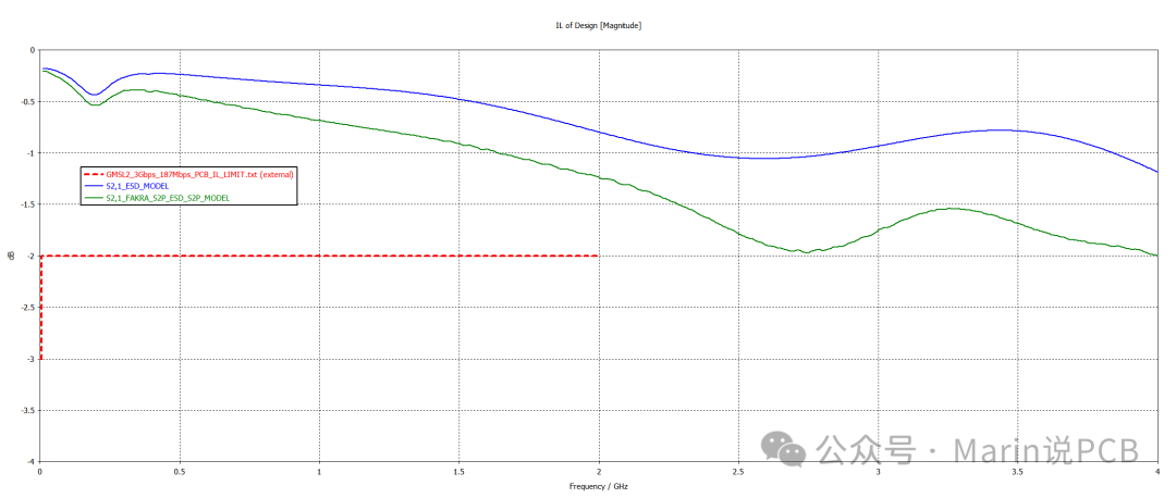
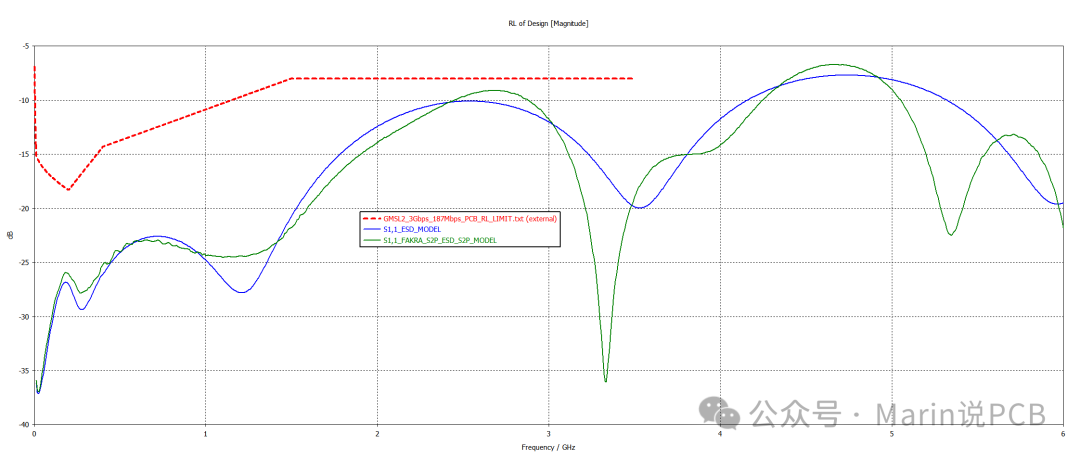
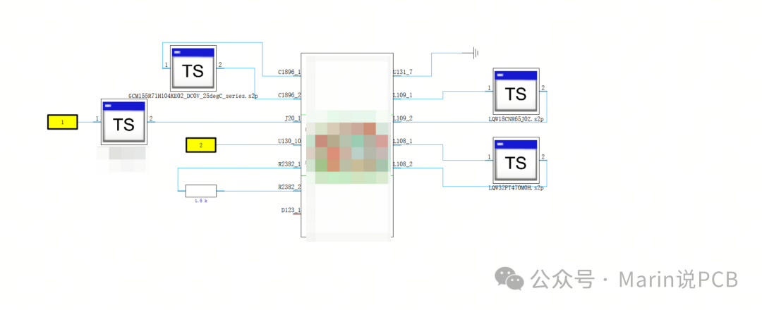
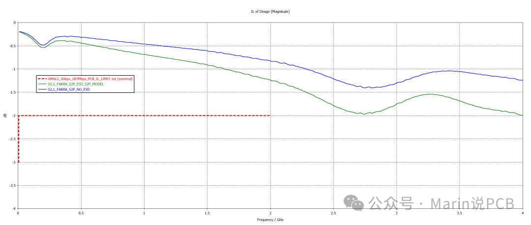
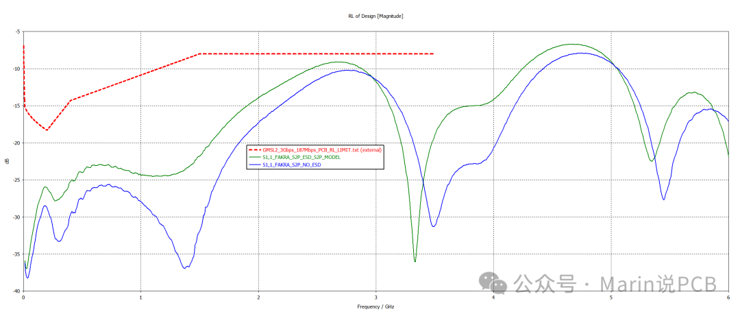
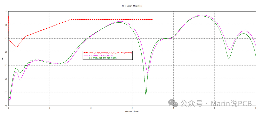
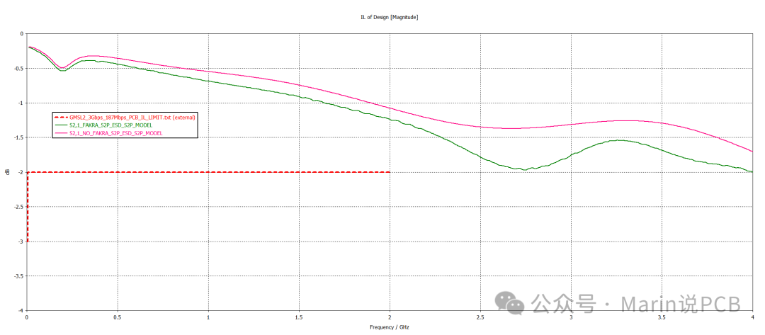
5. The S-parameter models of both devices are imported (the worst-case simulation scenario, which somewhat matches the actual measurement). Note: The FAKAR interface imports the actual S-parameter model of the device, and the ESD device also imports the actual S-parameter data model. Let’s look at its simulation results:
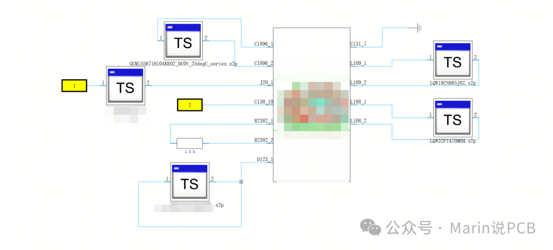 Editor
IL:
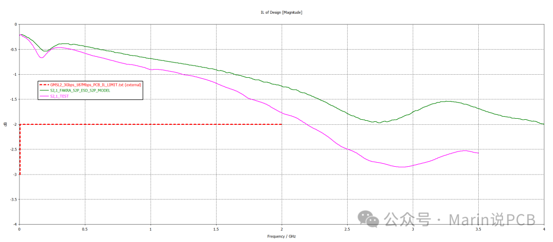 Editor
RL :
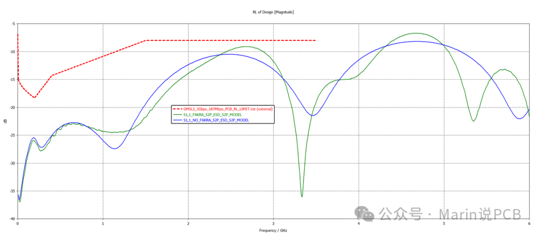 Editor
Note: This simulation case is the one that is closest to our actual test results; the overall trend matches the actual test results quite well, and it does not deviate significantly in the high-frequency range as before.
6. Only the S-parameter model data of the ESD device is imported, and the S-parameter model of the FAKAR interface is not imported, treated as an ideal 50-ohm impedance PORT. Let’s look at its simulation results:
 Editor
IL:
 Editor
RL :
 Editor
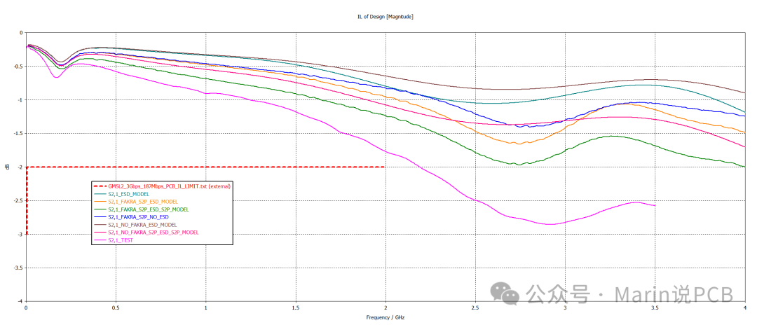
Let’s look at the overall simulation cases and the actual measurement results together:
IL:
 Editor
RL :
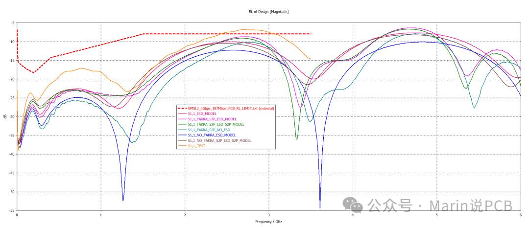 Editor
Conclusion: Through the above simulation comparisons, it can be seen that to obtain more accurate simulation data, it is best to include the S-parameter models of all devices in the network, as this will more realistically reflect the quality of signal propagation. This also reflects why our previous simulation design performed so well in the high-frequency range, as the actual S-parameter models of the devices (ESD and FAKAR) were not included.
Alright, everyone, that’s all for this issue. See you in the next article.
Editor
Editor
——– Disclaimer: This article belongs to the original work of the editor, please indicate the source if reprinted!