Editor’s Note: The content of this article is quite concise. The first two factors are introduced using ADS simulation schematics, and those interested can follow along. Many buses have requirements for loss, so for design engineers, it is essential to understand which factors dominate the changes in loss.
We often discuss the issue of loss in PCBs. Some engineers may ask, what factors affect the magnitude of loss? The most common answers usually mention the PCB material’s loss factor, the length of the PCB transmission line, and the roughness of the copper foil. However, the answers are certainly not limited to these. Below, we will conduct experiments on the corresponding parameters to introduce which factors influence transmission line loss in PCBs.
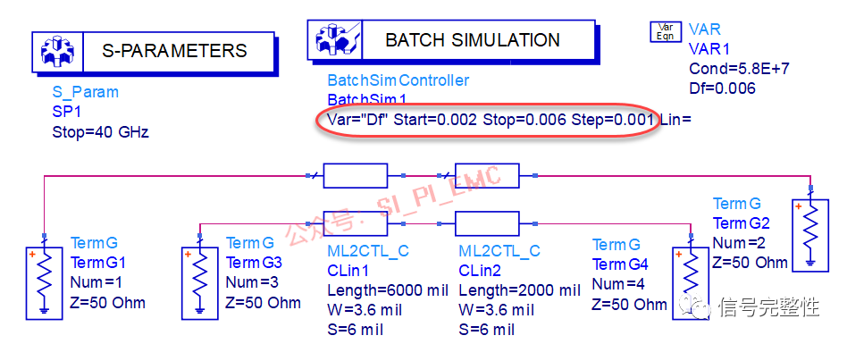
First, let’s look at the impact of the dielectric loss factor Df on loss. By analyzing the variation of Df as a variable, we can see its effect on loss. The following diagram illustrates the analysis schematic:
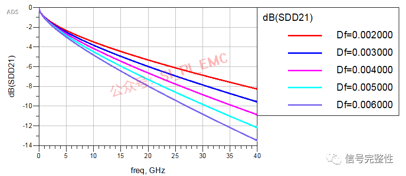
 The simulation comparison results are as follows. Clearly, as the dielectric loss factor Df increases, the loss also increases:
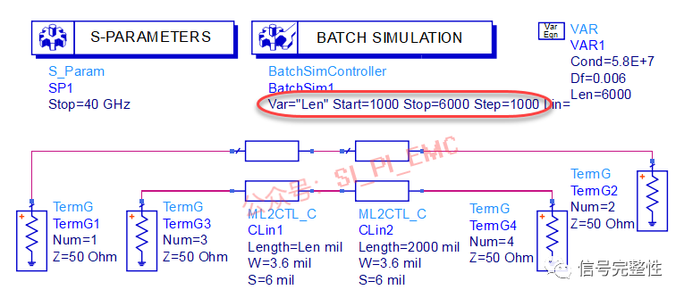
Length is also one of the main factors affecting loss. By setting the transmission line length as the variable Len, we analyze the effect of changes in Len on loss. The following diagram illustrates the analysis schematic:
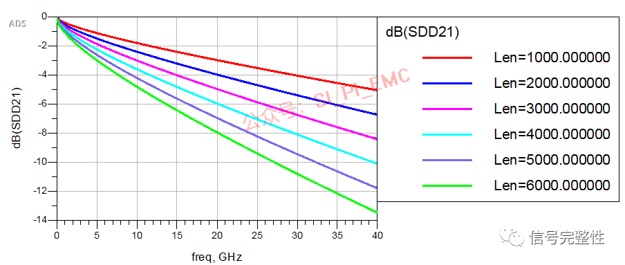
The simulation comparison results are as follows. Clearly, as the transmission line length increases, the loss also increases:
Copper foil is a commonly used conductor in PCBs, and its roughness also affects loss. The impact of roughness variation on loss is shown in the following diagram:
From the above diagram, we can see that as the roughness of the copper foil increases, the loss also increases.
These three influencing factors are easily understood by engineers. To reduce loss, engineers typically consider using low dielectric loss tangent materials, shortening transmission line lengths, and reducing copper foil roughness.
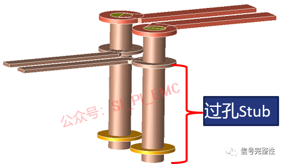
In addition to these three influencing factors, there are also factors such as vias, unequal lengths of transmission lines, and crosstalk that affect loss. For example, in high-layer boards, vias often have stub remnants, as shown in the following diagram:
Stub remnants can lead to increased loss. The following diagram shows the loss results for the same via, with and without stubs. When stubs are present, there is a significant resonance point, where the loss is very high.
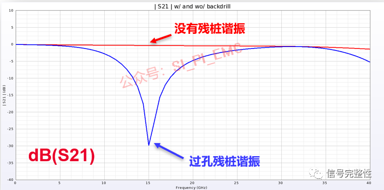
Moreover, as the stub length increases, the resonance frequency decreases (which corresponds to increased loss at specific frequencies).
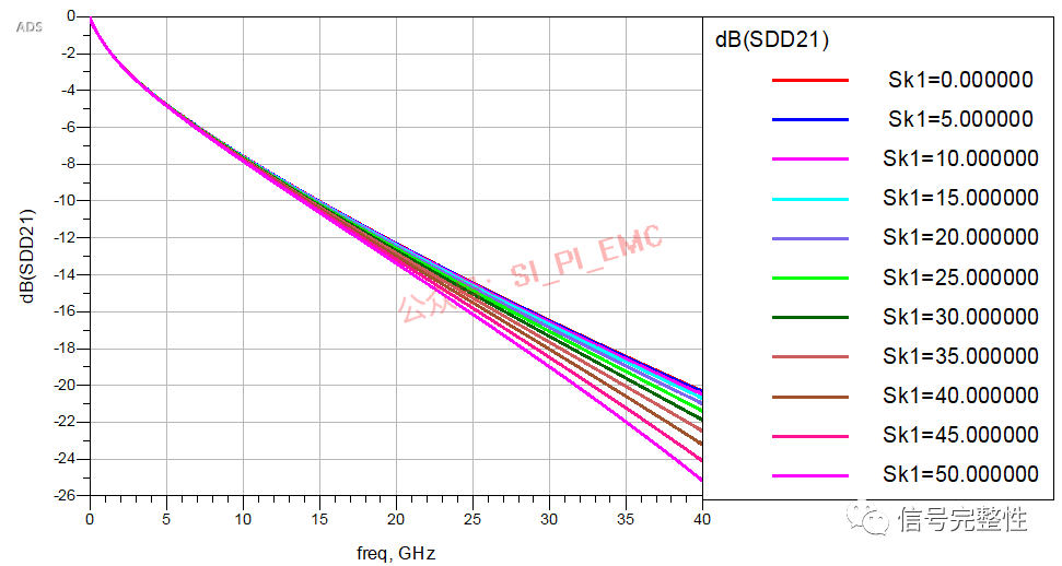
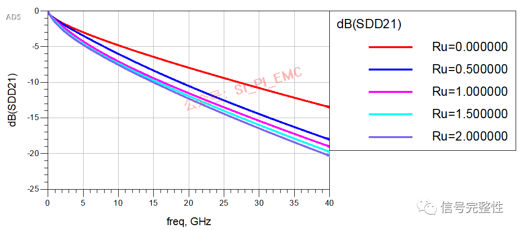
In PCB design, it is common to encounter unequal lengths in differential pairs (skew). Experiments have shown that as the skew length changes, the loss also varies. The following diagram illustrates that as the skew length increases, the loss at the same frequency point also increases.
In the design of increasingly integrated products, crosstalk is a concern for engineers. Severe crosstalk can lead to many signal integrity issues, one of which is its impact on loss. The following diagram shows the comparison of loss when the spacing between transmission lines changes in a microstrip line.
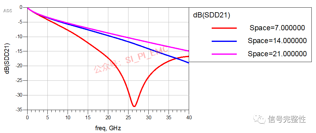
Clearly, when other settings remain unchanged, a larger spacing results in smaller loss attenuation at the same specific frequency point. In fact, there are some interesting phenomena regarding the impact of crosstalk on loss, such as when crosstalk causes resonance points of loss, etc.
The above factors have a significant impact on the loss of PCB transmission lines. Of course, there are other factors, and we will share experimental results on those in the future. Feel free to leave comments at the end of the article for further discussion.
[1]Driven by Interest and Passion
[2]Should Hardware Engineers Design Their Own PCBs?
[3]How Long Should PCB Traces Be??
[4]How Wide Should PCB Traces Be?
[5]Inner Layers of PCBs
[6]Vias
[7]Can PCBs Have Sharp Angles and Right Angles?
[8] Should Dead Copper Be Retained? (PCB Islands)
[9]Can Vias Be Placed on Pads??
[10] What Material Does FR4 Refer To?
[11] Why Is the Solder Mask Layer Usually Green?
[12]Steel Mesh
[13]Pre-layout
[14]Principles of PCB Layout and Routing
[15]Cross-Splitting Traces
[16]Signal Reflection
[17]Dirty Signals
[18]Surface Treatment Processes such as Gold Plating, Tin Spraying, etc.
[19]Trace Spacing
[20]Placement of Capacitors
[21]Crosstalk
[22]Flying Probe Testing of PCBs
[23]Overview and Simulation of FPC
[24] Why Do PCBs Deform and Bend? How to Solve It?
[25] Understanding “Characteristic Impedance” in One Article
[26] Layer Design of PCBs
[27] Reflow Path for High-Speed Circuit PCBs
[28] Power Handling and Plane Segmentation in PCB Design
[29] Zigzag PCB Traces – Tabbed Routing
[30] What Is the Dielectric Loss Angle in PCBs??
[31] The Impact of Copper Foil Roughness on High-Speed Signals
[32] Why Should Crystals Not Be Placed at the Edge of PCBs?
[33] What Are High-Speed Signals?
[34] What Is a Transmission Line?
[35]Pre-emphasis, De-emphasis, and Equalization
[36] How to Utilize PCB Heat Dissipation
[37]Stubs in PCB Design
[38] The Dilemma: Should There Be Ground Protection Traces Between Traces?
[39] PCB Copper Pour
[40] Rules to Follow When Designing PCBs
[41] The “Fake Eight Layers” in PCB Layer Design
[42] Besides Stripline and Microstrip, There Are Also “Co-planar Waveguides”
[43]Parameters Related to PCB Pad Design Processes
[44] Why Should Ground Holes Be Drilled on PCB Edges?
[45] PCBs That Are Easier to Dissipate Heat: Aluminum Substrates
[46]Why Should Reference Planes Be Hollowed Out?
[47] Crystal Oscillator PCB Design
[48] Designing PCB for DC/DC Power Supplies with EMC Considerations
[49] PCB Turns: Round Corners Are Not Always the Best Routing
[50] Why Should Vias Be Plugged? “Conductive Via Plugging Process”
[51]Key Points for Power PCB Layout and Routing
[52]Mark Points on PCBs
[53]Using ADS to Simulate High-Speed Signal Cross-Splitting
[54] Rigid-Flex PCBs
[55] Mixed Signal PCB Design
[56]Placement of Capacitors in PCB Design
[57] The Impact of Via Stubs in PCB Design
[58] Placement and Routing of Decoupling Capacitors in PCB Design
[59] PCB Design Checklist: Structure
[60] PCB Design Checklist: Power
[61] PCB Design Checklist: Routing
[62] PCB Design Checklist: High-Speed Digital Signals
[63] Process Edges
[64] PCB Design: Gold Fingers
[65]PCB Design: Differential Pairs
[66] PCB Design and Simulation for DDR4
[67] PCB Material Properties to Consider in Circuit Board Design
[68]What Constitutes Good “PDN” PCB Design?
[69] Detailed Layout and Routing Design for PCBs
[70]USB2.0 PCB Routing
[71] Key Points for Flyback Switch Power Supply PCB Design
[72] PCB Design: Pad and Via Process Specifications
——Recommended Hardware Books——