Click the blue text to follow us for regular updates.
01
Article Introduction
This article is a collaborative effort by research teams from Fudan University, Dalian University of Technology, and Peking University. It presents a novel ultrathin crystalline silicon-based omnidirectional strain sensor designed for implantable/wearable dynamic monitoring of soft tissue biomechanics in multiple directions. The sensor features a four-sensor “octopus” layout, combined with a 45° coordinate system theoretical model, enabling simultaneous detection of strain intensity and direction with an accuracy of approximately 1° in angular deviation and a minimum strain detection limit of 0.1%. The device exhibits biodegradability, high biocompatibility, and mechanical flexibility, making it suitable for intra-body diagnostics and pathological localization of cardiac diseases such as intraocular pressure monitoring, facial expression recognition, pulse wave detection, and myocardial infarction.
Journal: Science Advances
Title: Ultrathin crystalline silicon–based omnidirectional strain gauges for implantable/wearable characterization of soft tissue biomechanics
Corresponding Authors: Mei Yongfeng, Song Enming from Fudan University; Han Mengdi from Peking University; Li Rui from Dalian University of Technology.
02
Fabrication Method
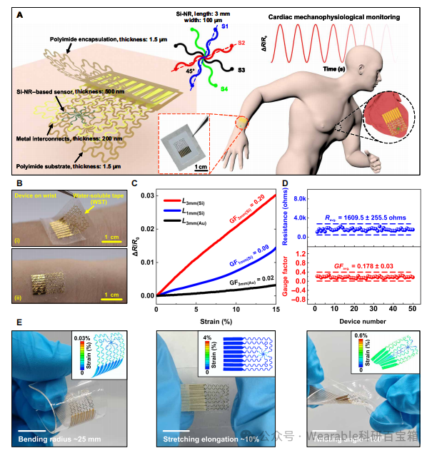
Fig. 1. Design and working mechanism of the CUISD.
1
Core Material Preparation: Silicon Nanobelt
① Starting Material: Use an Insulator on Silicon Wafer (SOI wafer), structured from top to bottom as: device layer silicon (500 nm thick) / silicon dioxide sacrificial layer (1 μm thick) / silicon substrate.
② Doping: Boron doping of the top silicon layer of the SOI wafer (960°C, 15 minutes) to achieve suitable conductivity (p-type, concentration approximately 10²⁰ atoms/cm³), which is fundamental for forming the piezoresistive sensor.
③ Release of Silicon Film: Etch away the intermediate silicon dioxide sacrificial layer using hydrofluoric acid (HF) solution to separate the ultrathin single-crystal silicon film from the bottom silicon substrate.
④ Transfer Printing: Use a PDMS stamp to “pick up” and “print” the released ultrathin silicon film onto a temporary flexible substrate (polyimide, PI).
2
Device Patterning and Integration
① Photolithography and Etching: Define four serpentine silicon nanobelts arranged in an “octopus” radial pattern on the silicon film transferred to the PI substrate through photolithography and reactive ion etching processes. Each sensor is 3 mm long and 100 μm wide, with adjacent sensors spaced at a 45-degree angle.
② Metal Interconnection: Deposit a chromium/gold (Cr/Au, 10/200 nm) layer through magnetron sputtering, followed by photolithography and wet etching to form serpentine metal wires connecting the four silicon sensors.
③ Packaging: Spin-coat an additional layer of polyimide (PI, approximately 1.5 μm thick) on top of the device as a packaging layer to protect the device. At this point, the sensor structure is sandwiched between the upper and lower layers of PI, forming a “sandwich” structure.
④ Formation of Mesh Structure: Pattern the entire device area through photolithography and etching to create an open mesh structure, significantly enhancing the mechanical flexibility and stretchability of the device during stretching and bending.
3
Device Release and Mounting
① Sacrificial Layer Dissolution: Immerse the entire sample in acetone to dissolve the initially coated polymethyl methacrylate (PMMA) sacrificial layer on the glass substrate.
② Release of Finished Product: The device is released from the rigid glass substrate, becoming an independent ultrathin (total thickness < 4 μm), flexible film device.
③ Mounting: Using water-soluble tape (WST) or biological glue, the device can be conveniently and securely attached to the surface of biological tissues such as skin and heart.
4
Fabrication of Biodegradable Version
To create an implantable and biodegradable version, key material substitutions were made in the fabrication process:
① Metal Interconnection: Replace non-biodegradable gold (Au) with biodegradable molybdenum (Mo).
② Substrate and Packaging: Replace polyimide (PI) with biodegradable dynamic covalent polyurethane (b-DCPU).
③ Process: After the device is completed on the temporary substrate, it is sandwiched between two layers of b-DCPU film (each 50 μm thick) and finally released from the substrate through an electrochemical delamination method, forming a fully biodegradable implantable sensor.
03
Original Illustrations
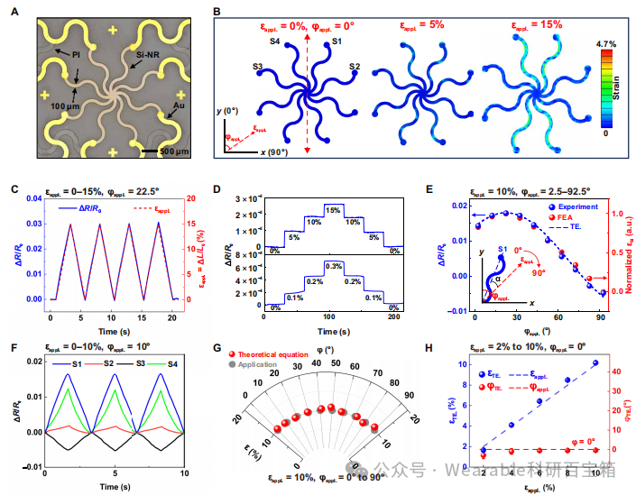
Figure 2. Multilayered Ag NF electrode for the CUISD.
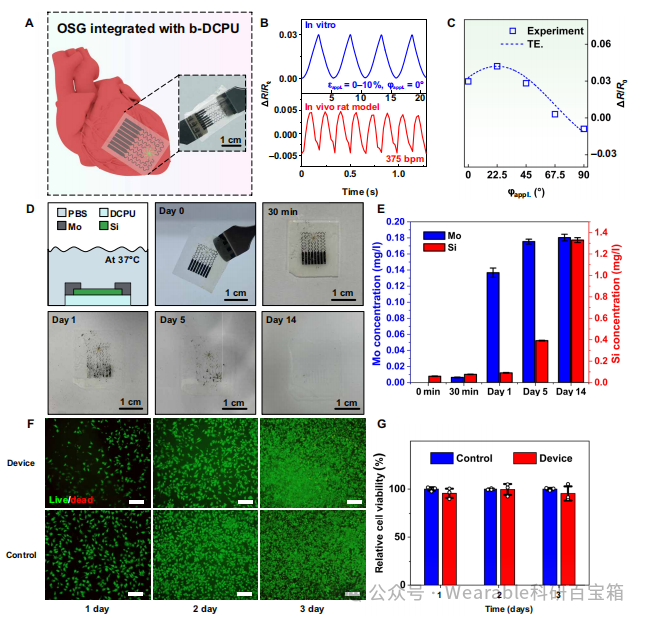
Fig. 3. Fabrication and characterizations of the CUISD.
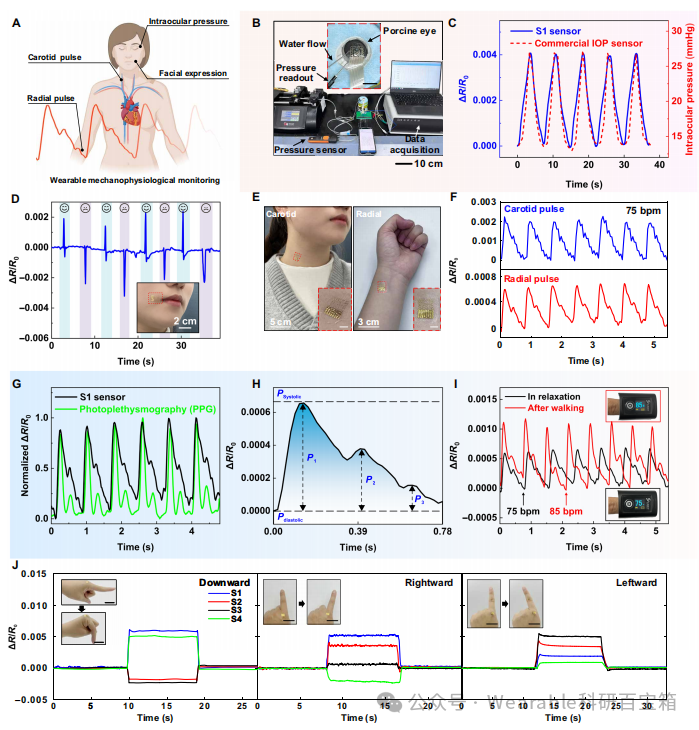
Figure 4. CUISD for dynamic display and motion tracking.
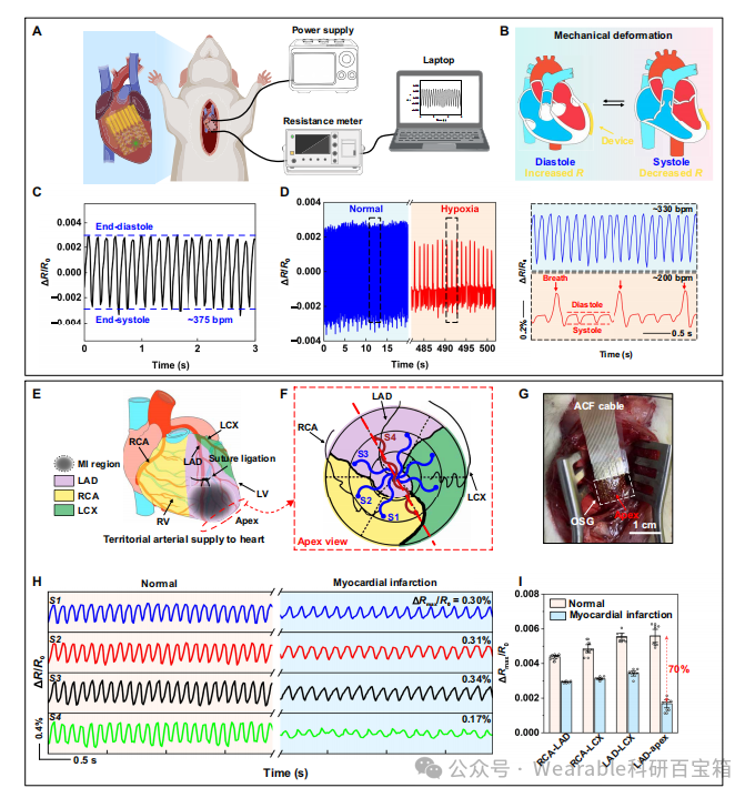
Figure 5. CUISD for breath-based interaction systems.
04
Materials and Equipment (Partial)
|
Material |
Function |
Supplier |
|
SOI Wafer |
Provides single-crystal silicon device layer |
SOITEC |
|
Photoresist S1805 |
Photolithography process |
Dow (Dow Chemical) |
|
Polyimide |
Flexible substrate and packaging layer |
Changzhou Yaan New Materials |
|
Polymethyl Methacrylate |
Sacrificial layer |
Microchem (950 PMMA A7) |
|
Kapton Film |
Temporary substrate for transferring biodegradable devices |
DuPont |
|
Water-Soluble Tape |
Device transfer and mounting |
3M (5414 Transparent Tape) |
|
Biological Glue |
Adhesive for attaching devices to skin |
Smooth-On Inc. (Derma-tac) |
|
Photolithography Machine |
Transfers circuit patterns to substrates |
SUSS (MAG) |
|
Reactive Ion Etching Machine |
Dry etching of silicon and polyimide |
Trion (T2) |
|
Magnetron Sputtering System |
Deposits metal films (Cr/Au, Mo) |
DE Technology (DE500) |
|
Motorized Displacement Stage |
Applies controllable tensile strain |
Dongyuan Chuanghui (DYCH-57H568S) |
|
Electrochemical Workstation |
Measures resistance changes of sensors |
CH Instruments Inc. (CHI660e) |
|
Pressure Sensor |
Measures intraocular pressure as a reference |
Testo (510i) |
|
Heart Rate Monitor |
Pulse monitoring comparison |
LEPU (Lepu Medical: PC-60F) |
For more information on materials and equipment, feel free to contact us!
The literature shared has been credited to the authors and sources; please contact us for removal if there are any infringements! Any errors are welcome to be pointed out in the comments!
END


Business Cooperation | Technical Consultation
Material Issues | Equipment Issues
Like and follow us for more articles and information…