1. Problem Description:
In ADC sampling circuits, especially in low-power product battery voltage sampling circuits, larger voltage divider resistors are typically chosen. This helps to reduce the additional power consumption caused by the voltage divider circuit. However, this can lead to inaccurate voltage sampling.
2. Problem Analysis
When the ADC samples a single-ended voltage, if the sampled voltage is not strongly driven (with very low current), the charging time of the internal sampling capacitor of the ADC will increase (manifesting as a longer rise time). For voltage sampling generated by large resistor dividers, the capacitor charging effect at this time will affect the sampling voltage (the internal sampling capacitor of the ADC is approximately 15pF), resulting in a voltage spike that pulls down the sampling voltage at the moment of sampling, as shown in Figure 2-1. This can easily lead to a significantly erroneous value.
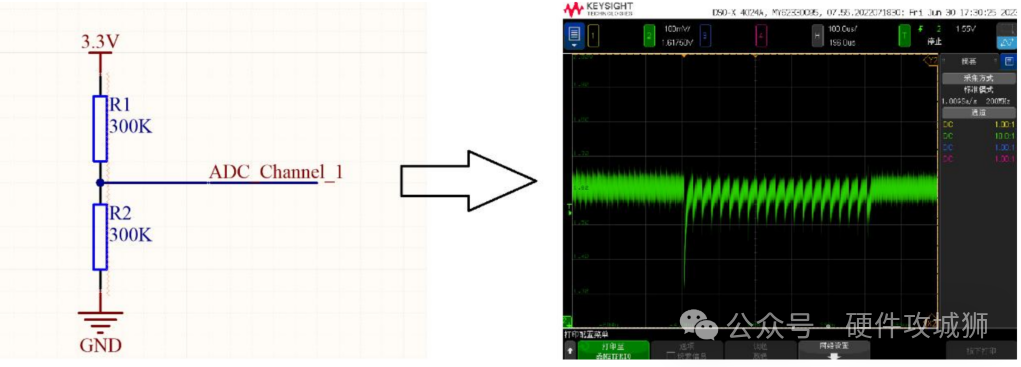
Figure 2-1 The effect of internal capacitance on low-drive sampling circuits
This effect increases with the value of the voltage divider resistor.
3. Solution:
Add a capacitor to the ground side of the voltage divider resistor, typically 0.1uF, as shown in Figure 2-2. The principle is to buffer the current by adding a capacitor, thereby eliminating voltage spikes caused by insufficient current.
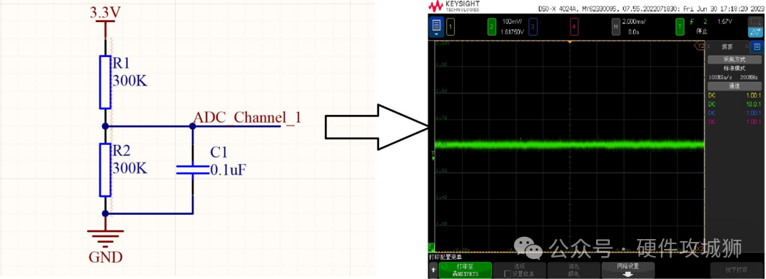
Figure 2-2 Improvement of ADC sampling circuit after adding a capacitor
4. Other Derivative Issues
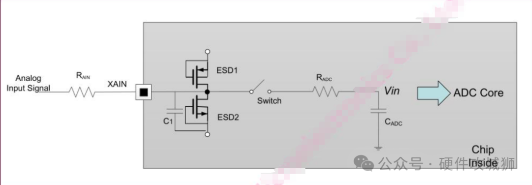
The equivalent parasitic resistance of the sampling input circuit should not be too large. The equivalent sampling circuit is shown in Figure 2-3. The equivalent parasitic resistance needs to meet the following equivalent formula requirements:
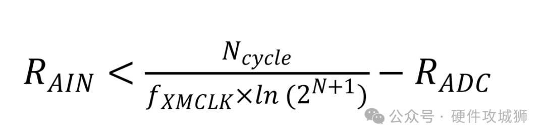
Note: This formula is an ideal calculation formula, and specific situations need to be determined based on the actual product design.
Where RADC typical value is 350Ω, CADC typical value is 15pF, fXMCK is the ADC operating frequency, Ncycle is the sampling period (in ADC clock cycles), and N is the number of conversion cycles.
For a sampling rate of 2MSPS, the conversion time is approximately 12.5 clock cycles, and the minimum sampling time is 1.5 cycles (i.e., Ncycle = 1.5), with N taken as 12. In this case, the main frequency is 28MHz (i.e., fXMCLK = 28MHz). After calculation, RAIN can be set to 46.3Ω.
 — End —
Disclaimer: This account maintains neutrality regarding all original and reprinted articles’ statements and viewpoints. The articles are provided solely for readers’ learning and communication. The copyright of the articles and images belongs to the original authors. If there is any infringement, please contact for removal.
Recommended Reading:PCB Layout Techniques for TVS Diodes7 Common MOSFET Gate CircuitsWhy Are Resistors Often 4.7kΩ or 5.1kΩ Instead of Whole Numbers Like 5kΩ?Summary: MOSFET SOA Failure, Avalanche Failure, and dV/dt Failure6 Types of Delay Circuits ExplainedSpike Suppression – Design Methods for Buffer CircuitsUnderstanding Ceramic Capacitors in One Article