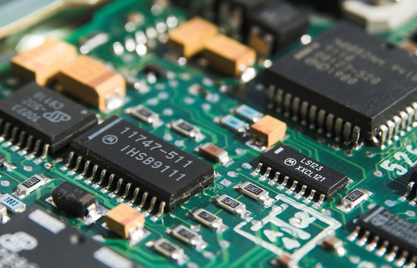
Printed Circuit Boards (PCBs) are the core components in electronic devices, playing a crucial role in connecting and transmitting electrical signals. The manufacturing process is complex and surprising, with each step significantly impacting the performance and reliability of the final product. Therefore, engineers must be well-acquainted with the PCB manufacturing process. This article will discuss the PCB production process in detail, hoping to assist everyone.

Generally speaking, the PCB manufacturing process can be divided into: trimming the board’s dimensions – copying – drilling positioning holes – applying adhesive – etching – cleaning – removing adhesive – polishing with fine sandpaper – applying rosin solution.
1. First, polish the surface of the copper-clad board that meets the size requirements with fine sandpaper, then use transfer paper to copy the wiring diagram onto the copper-clad board.
2. Use a 1.0 mm diameter drill bit to drill positioning holes, and then apply adhesive (or paint).
3. After applying the adhesive, place a thick sheet on the board and press down with your palm. This is to ensure that the adhesive adheres more firmly to the copper-clad board. If necessary, a hairdryer can be used for heating to enhance the adhesive’s viscosity. Since the adhesive used has good stickiness and the adhesive tape is thin, this method works well, and generally, no additional heating treatment is needed.
4. Etching generally uses ferric chloride as the etching solution. The etching speed is related to the concentration of the etching solution, the temperature, and the shaking during the etching process. To ensure the quality of the board and improve the etching speed, shaking and heating methods can be employed.
5. After etching, rinse the board thoroughly with tap water, remove the adhesive tape, and dry the printed board.
6. Use fine sandpaper to polish the copper surface of the printed board until it is shiny, and then immediately apply the rosin solution. (When applying the rosin solution, the printed circuit board should be tilted to avoid the rosin flowing through the drilled holes to the back.)
This article is an original piece by Yiy Education. Please indicate the source when reprinting!