Detailed Explanation of the LT2500-32 32-bit ADC Data Sheet.1
Hang in there, the upcoming article is very exciting!
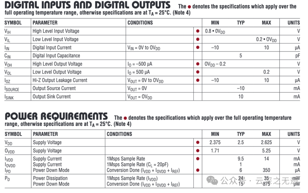
Digital input/output characteristics. Used to evaluate level compatibility, current driving capability, etc. when connected to MCU or FPGA:
| Parameter | Description | Condition | Min | Typical | Max | Unit | Interpretation |
|---|---|---|---|---|---|---|---|
| VIH | High-level input threshold | – | 0.8×OVDD | – | – | V | Digital input > 80% OVDD is recognized as high |
| VIL | Low-level input threshold | – | – | – | 0.2×OVDD | V | < 20% OVDD is low |
| IIN | Input leakage current | VIN: 0V–OVDD | -10 | – | 10 | µA | Very small, compatible with any logic |
| CIN | Input capacitance | – | – | 5 | – | pF | Minor load effect on high-speed signals |
| VOH | High-level output | IO = –0.5 mA | OVDD – 0.2 | – | – | V | Output logic high pulled close to OVDD |
| VOL | Low-level output | IO = 0.5 mA | – | – | 0.2 | V | Output low level close to 0V |
| IOZ | High impedance output leakage current | In tri-state | –10 | – | 10 | µA | Used for SPI tri-state output detection |
| ISOURCE | Pull-up current capability | When outputting high | -10 | – | – | mA | Maximum pull-up current 10 mA (source) |
| ISINK | Sink current capability | When outputting low | – | – | 10 | mA | Maximum sink current 10 mA |
SPI communication can be compatible with 1.8V, 3.3V, and 5V systems, as long as OVDD corresponds; SDOA / SDOB output pins can directly drive 10mA receivers, such as FPGA inputs; level logic is compatible with CMOS/TTL devices.
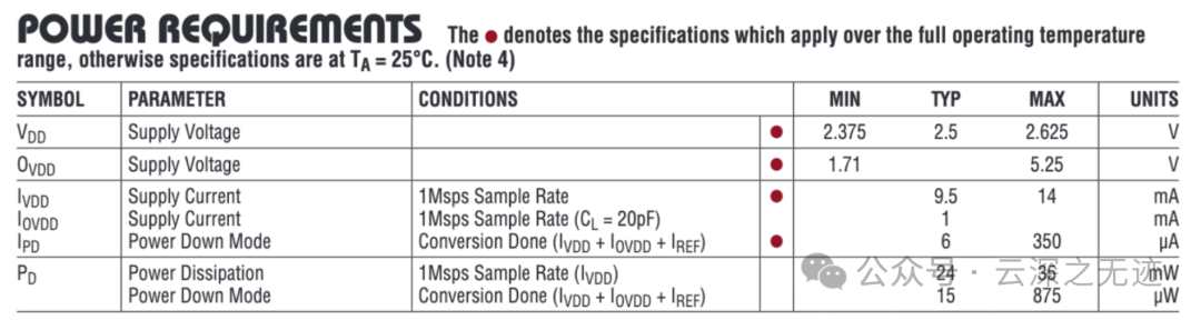
Power supply requirements
| Parameter | Description | Condition | Min | Typical | Max | Unit | Interpretation |
|---|---|---|---|---|---|---|---|
| VDD | Analog core power supply | – | 2.375 | 2.5 | 2.625 | V | Requires stable 2.5V LDO power supply |
| OVDD | Digital IO power supply | – | 1.71 | – | 5.25 | V | High flexibility, compatible with 1.8V~5V systems |
| IVDD | Analog current | 1Msps sampling rate | – | 9.5 | 14 | mA | Analog front-end power consumption |
| IOVDD | Digital current | 1Msps, CL=20pF | – | 1 | – | mA | IO section driving consumption |
| IPD | Shutdown current | After sampling is complete | 6 | – | 350 | µA | Current in sleep state |
| PD | Power consumption | At full-speed sampling | – | 24 | 35 | mW | Total power consumption (analog + digital) |
| Power-down mode | – | 15 | 875 | µW | Very suitable for low-power sampling strategies (e.g., intermittent) |
Maximum power consumption at full-speed sampling (1Msps) is about 35mW, very suitable for portable high-precision systems; if the power-down mechanism is enabled, power consumption can be as low as several tens of microwatts; OVDD is flexible, suitable for various interface logic level compatibility.
The ADC has two power supply parts:
| Power Channel | Name | Voltage | Main Function | Power Supply Requirements |
|---|---|---|---|---|
| VDD | Analog core power | 2.5 V | Supplies the internal analog circuits of the ADC (sample and hold, reference amplifier) | Must be extremely low noise, stable, and ripple-free |
| OVDD | Digital IO power | 1.8 V / 3.3 V / 5.0 V | Supplies SPI, BUSY, SDO, SDI, and other digital interfaces | Matches the logic level of the main MCU/FPGA |

       +5V system power input (battery/USB/Vin/DC-DC)
                  │
         ┌────────┴────────┐
         │                 │
    Precision LDO            Low Noise LDO / LDO Output
     (VDD power)            (OVDD power)
     Output 2.5V              Output 3.3V
     10µV RMS low noise        Matches MCU / FPGA levels
         │                      │
    ┌────▼────┐           ┌────▼────┐
    │ LTC2500 │           │ Main Control Chip │
    └─────────┘           └─────────┘
The VDD power of the LTC2500 must be clean, wired separately, and away from switching interference; it is recommended that REF and VDD power share the same low-noise LDO; GND grounding must be single-point converged to avoid mixing of digital and analog return flows; it is recommended to use partitioned ground + π-type filter (L-C-L) to further clean the power supply; if there is a switching power supply in the system (such as Buck), it must be kept away from the ADC area and filtered with LDO in advance.
Power Budget Reference
| Item | Current Consumption (Typical) | LDO Current Capability |
|---|---|---|
| VDD | 9.5 mA | ≥ 50 mA, with margin |
| OVDD | 1 mA (normal IO) | ≥ 20 mA |
Overall Power Supply System Solution Summary
One path is for the analog part of the ADC, which needs to be low noise, and the other is for the digital part, which is not as picky.
| Module | Recommended Device | Characteristics | Usage |
|---|---|---|---|
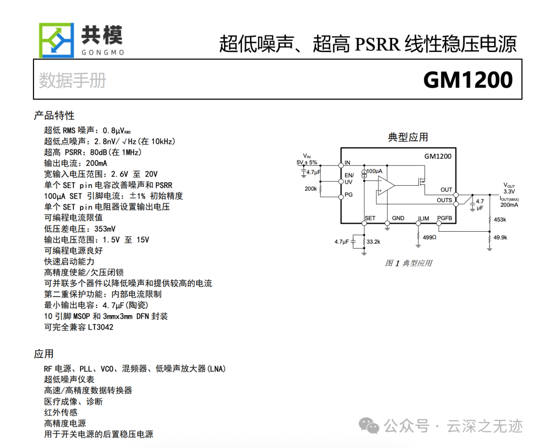
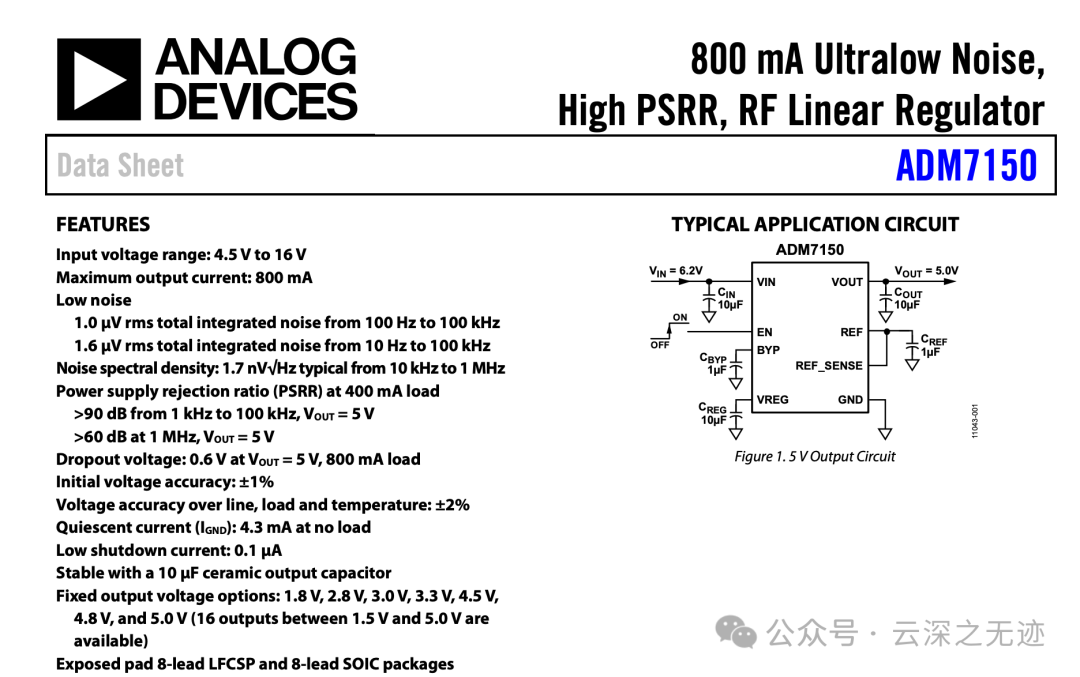
| LDO1 | LT3042 / ADM7150 | Extremely low noise | LTC2500 VDD & REF |
| LDO2 | LP5907 / MIC5365 | Logic compatible | LTC2500 OVDD |
| Upstream Power Supply | 5V DC or lithium battery / Buck conversion | Input voltage | Main power supply for the system |
Continue reading:
 Includes key indicators such as sampling rate, clock requirements, and data output timing.
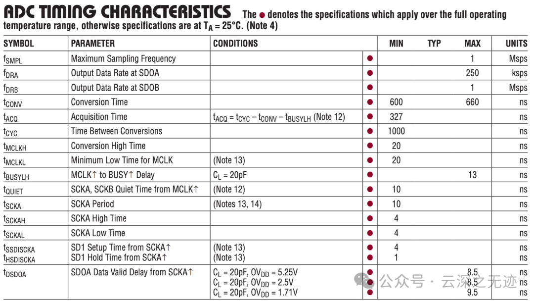
Sampling and Conversion Related Parameters
| Symbol | Parameter | Typical Value | Unit | Description |
|---|---|---|---|---|
| fSMPL | Maximum sampling frequency | 1 | Msps | Highest supported main clock sampling rate (MCLK) of 1Msps |
| fDRA | SDOA output data rate | 250 | ksps | Affected by the filter (slower when DF is large) |
| fDRB | SDOB output data rate | 1 | Msps | SDOB outputs data on every sample, matching the sampling frequency |
| tCONV | Conversion time | 600–660 | ns | How long it takes to complete the conversion after the MCLK rising edge |
| tCYC | Minimum time between two samples | 1000 | ns | Minimum period limit = 1Msps |
| tACQ | Acquisition time (sample and hold) | ≥ 327 | ns | Derived from the formula:<span>t_ACQ = t_CYC - t_CONV - t_BUSYLH</span> |
| tBUSYLH | Delay from MCLK↑ to BUSY↑ | 13 | ns | Can be used to synchronize to determine if sampling is complete |
MCLK Clock Requirements (Main Sampling Clock)
| Parameter | Value | Unit | Description |
|---|---|---|---|
| tMCLKH | High level time | ≥ 20 | ns |
| tMCLKL | Low level time | ≥ 20 | ns |
The maximum frequency of MCLK is approximately:
However, since the conversion process and sampling timing are independent, the MCLK rising edge only triggers the event, and the internal timing is independent of the MCLK frequency.
SPI (SDOA/SDOB) Interface Timing
| Parameter | Value | Unit | Description |
|---|---|---|---|
| tSCKA | SPI SCKA period | ≥ 10 | ns |
| tSCKAH | SCK high level | ≥ 4 | ns |
| tSCKAL | SCK low level | ≥ 4 | ns |
| tSSDISCKA | SDI data setup time | ≥ 4 | ns |
| tHSDISCKA | SDI data hold time | ≥ 1 | ns |
| tDSDOA | SDOA data valid delay | 8.5 / 8.5 / 9.5 | ns |
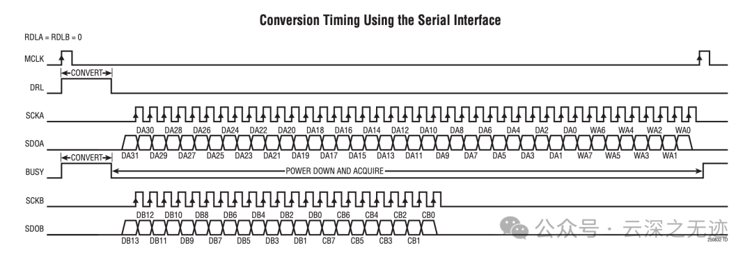
- MCLK rising edge → Triggers a sample;
- BUSY goes high → Indicates the ADC is working;
- BUSY goes low → Data is readable (DRL goes low);
- The SPI master controls reading through SCKA/SCKB + SDI;
- SDOA/SDOB outputs data, meeting the above timing requirements.
Compatible with STM32 SPI mode 0; SCK ↑ samples, MSB first
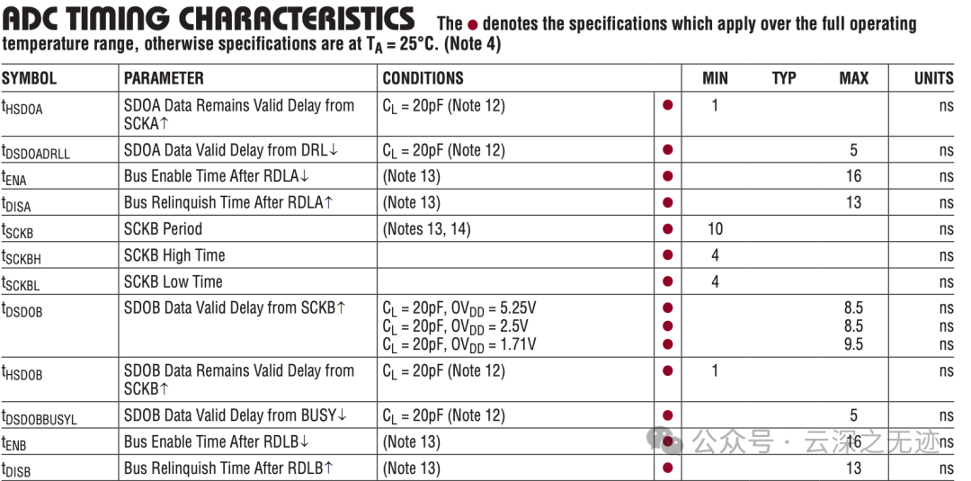
SPI Read Timing Indicators (SDOA / SDOB)
| Symbol | Parameter Description | Condition | Min | Unit | Description |
|---|---|---|---|---|---|
| tHSDOA | SDOA data hold time from SCKA↑ | CL=20pF | 1 | ns | Latest time for the SPI master to sample SDOA |
| tDSDOADRL | SDOA data valid delay after DRL goes low | – | 5 | ns | Indicates when the filtered data can be read |
| tENA | RDL alling to bus enable time | – | 16 | ns | Used for controlling timing when parallel chip select |
| tDISA | RDL aising to bus release time |
– | 13 | ns | Time needed to hold during SPI bus release (CS cancellation) |
| tSCKB | SPI clock period for SDOB | – | 10 | ns | SPI clock period ≥10ns, i.e., maximum 100 MHz |
| tSCKBH | SDOB SCKB high level time | – | 4 | ns | |
| tSCKBL | SDOB SCKB low level time | – | 4 | ns |
No Delay Output SDOB Specific Timing Parameters
| Symbol | Parameter Description | Condition | Value | Unit | Description |
|---|---|---|---|---|---|
| tDSDOB | SDOB output valid delay after SCKB↑ | OVDD = 5.25V / 2.5V / 1.71V | 8.5 / 8.5 / 9.5 | ns | The lower the voltage, the slower the driving speed (longer delay) |
| tHSDOB | SDOB data hold time | CL=20pF | 1 | ns | Must hold for at least 1ns when the SPI controller reads |
| tDSDOBBUSY | SDOB output data valid after BUSY goes low | – | 5 | ns | BUSY signal can be used to trigger read operations |
Bus Chip Select Timing (RDLA/RDLB Control)
These are used to control multiple ADCs sharing the SPI bus (RDLA/RDLB are the SPI chip select pins)
| Parameter | Description | Minimum Value | Unit |
|---|---|---|---|
| tENA | RDL↓ to bus drive time | 16 | ns |
| tDISA | RDL↑ to release bus time | 13 | ns |
Function: Prevent multiple LTC2500s from driving the bus simultaneously, causing conflicts.
Notes Summary (Key Notes)
| Note Number | Content Summary |
|---|---|
| Note 4 | Typical conditions: VDD=2.5V, OVDD=2.5V, VREF=5V, fSMPL=1 MHz |
| Note 8 | Integral non-linearity (INL) is defined as the maximum deviation measured from the quantization centerline |
| Note 9 | Bipolar zero error = output fluctuates around ±0.5LSB; full-scale error = maximum deviation under ±FS conditions |
| Note 10 | All dB metrics refer to ±5V differential input |
| Note 11 | Increasing sampling rate → IREF current increases linearly |
| Note 12 | Some timing values are design guarantees, not batch tested |
| Note 13 | Bus chip select related parameters tested only at OVDD = 2.5V & 5.25V |
| Note 14 | tSCKA/tSCKB minimum 10ns, supports 100MHz SPI |
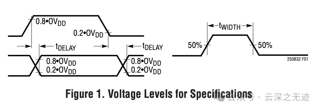 The image explains:
Input levels: Logic high ≥ 0.8×OVDD, logic low ≤ 0.2×OVDD; timing measurement points (50% level); tDELAY, tWIDTH, tSETUP, tHOLD etc. are standard digital timing definitions.