The chip packaging testing phase aims to process wafers that meet quality standards through precise cutting, wire bonding, and encapsulation processes to ensure electrical connections between the chip’s internal circuits and external devices, providing necessary mechanical and physical protection for the chip. Testing tools are used to conduct comprehensive and rigorous functional and performance testing on the completed packaged chips. The process of obtaining IC chips involves a complex workflow from design to manufacturing. Given their small and thin characteristics, chips are easily susceptible to scratches and damage if not properly protected. Packaging and testing serve to place, secure, seal, protect the chip, and enhance thermal performance, acting as a bridge between the internal world of the chip and external circuits—the contacts on the chip are connected to the pins of the packaging through wires, which in turn connect to other devices via traces on the printed circuit board. Therefore, packaging and testing play a crucial role in the field of integrated circuits.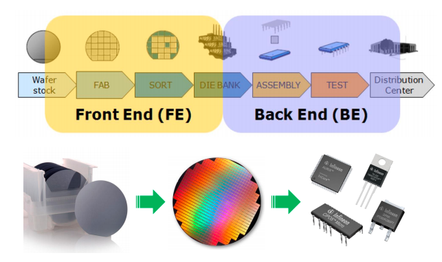 From Die to Finished ChipNext, we will provide a detailed introduction to the chip packaging testing process: From Die to Finished ChipNext, we will provide a detailed introduction to the chip packaging testing process:
Wafer Testing
Before further processing, integrated circuit wafers must undergo strict testing to ensure the functional integrity of the dies. The testing categorizes dies into three types: Good Die (functionally intact), Defective Die (with defects), and Fail Die (completely non-functional). Based on the classification requirements for product shipment, we select the dies that meet the criteria for the next specific packaging production step. This process is known as CP testing, which stands for Chip Probing Test, where probes connect to the pads of the dies for testing to ensure their functionality. This step is crucial for ensuring the quality of the final product.CP testing primarily relies on ATE testing machines (Automatic Testing Equipment, used to provide the necessary power, signals, and functional vectors for chip testing, and to receive output feedback signals from the chip to determine results), prober (a high-precision machine platform used to carry and move wafers so that the probe card’s probes can accurately contact and connect with the pads of the die), and probe cards (customized testing boards based on the circuit and testing requirements of each chip to achieve interconnection between ATE device channel resources and the chip’s corresponding pads). These devices and components work together to gradually complete the testing and verification of each die on the wafer. For dies with issues, they are typically marked on the surface using methods such as “ink dotting” for easy selection and identification during the subsequent packaging production process.
Chip Packaging (Assembly)
Through the CP testing of IC wafers, the subsequent packaging production of functionally normal dies can effectively avoid the cost losses associated with packaging defective chips. Although sometimes a “blind packaging” strategy is employed, where all dies on the wafer are packaged without undergoing CP testing, and testing and screening are conducted in later stages. However, this method is typically limited to early engineering batch wafers after chip tape-out, aimed at quickly obtaining engineering samples to verify the success of the tape-out chips, thus saving project time. In actual large-scale production phases, CP testing is an indispensable step.The chip packaging process varies significantly depending on the final packaging form of the finished chip. Taking the common wire bonding ball grid array packaging (WB-BGA) as an example, its production process encompasses the main steps of chip packaging.Wafer cutting is an extremely delicate and strictly demanding technical process aimed at dividing the wafer that has undergone CP testing into individual dies. In this process, a preliminary quality inspection of the wafer is first required to ensure it meets cutting requirements. Subsequently, a protective blue film is applied to the front of the wafer to prevent damage to the dies during cutting. Depending on the packaging size and heat dissipation requirements, the wafer may also need to be thinned, which involves reducing its thickness through mechanical grinding. Next, using diamond blades or laser cutting technology, the wafer is precisely cut along pre-set grooves (wafer scribing, which are reserved areas during wafer manufacturing to protect the dies during cutting). After this step, individual dies can be obtained. The wafer cutting process requires extremely high precision, as any minor process error can directly affect the quality of the dies. Therefore, this process relies on specialized production equipment—a wafer dicing machine. Globally, well-known wafer dicing machine manufacturers include Japan’s DISCO and ACCRETECH, as well as the American company Slicingtech. In China, companies like Jing Sheng Machinery and the 45th Institute of China Electronics Technology Group have also achieved significant accomplishments in this field.In the process of manufacturing the final chip, the substrate (Substrate, abbreviated as SUB) plays a crucial role. It is a special type of printed circuit board (PCB), whose key function is to extend the connection of the die’s pad pins to the ball pins after packaging. Therefore, the design and manufacturing of the SUB must be based on the specific conditions and packaging size of each chip. Currently, well-known SUB manufacturers in the industry include Japan’s Kyocera, Taiwan’s Nanya, Unimicron, and Kingboard. In mainland China, companies like Xingsen Technology, Zhuhai Yuya, Shenzhen South Circuit, and Shengyi Electronics are also actively working to break through the production technology of SUBs required for high-end chip packaging. Various SUBs (Chip Side and Ball Side)Substrate forms the foundational structure of chip packaging, similar to the foundation of a building. Subsequently, the die is precisely placed on one side of the substrate, a process known as Die Attach. The connection between the die and the substrate is achieved through fine wire bonding technology. To ensure the stability and safety of the chip, a metal protective lid is installed, a process known as Lid Attach. This protective lid is usually made of an alloy with excellent heat dissipation properties. On the other side, solder balls are installed on the chip, a process known as Solder Ball Mount. Then, through advanced reflow soldering technology, a solid connection between the solder balls and the SUB is ensured. At this point, the basic structure of the chip packaging is complete.After packaging is completed, the chip undergoes strict quality inspection. This includes using X-Ray and other technical means to conduct detailed inspections of the internal structure of the packaged chip to ensure packaging quality. Additionally, marking operations are performed, where the manufacturer’s logo, product name, production batch, and other information are laser printed on the surface of the chip. Once all quality indicators are confirmed to be qualified, the chip enters the baking process, known as Baking. This step aims to eliminate moisture and other factors in the packaging materials that may affect chip performance, ensuring that the chip exhibits stable and reliable characteristics in subsequent electrical performance work.Through this series of meticulous packaging process production steps, the original wafer die ultimately transforms into a finished chip, laying a solid foundation for subsequent applications. Various SUBs (Chip Side and Ball Side)Substrate forms the foundational structure of chip packaging, similar to the foundation of a building. Subsequently, the die is precisely placed on one side of the substrate, a process known as Die Attach. The connection between the die and the substrate is achieved through fine wire bonding technology. To ensure the stability and safety of the chip, a metal protective lid is installed, a process known as Lid Attach. This protective lid is usually made of an alloy with excellent heat dissipation properties. On the other side, solder balls are installed on the chip, a process known as Solder Ball Mount. Then, through advanced reflow soldering technology, a solid connection between the solder balls and the SUB is ensured. At this point, the basic structure of the chip packaging is complete.After packaging is completed, the chip undergoes strict quality inspection. This includes using X-Ray and other technical means to conduct detailed inspections of the internal structure of the packaged chip to ensure packaging quality. Additionally, marking operations are performed, where the manufacturer’s logo, product name, production batch, and other information are laser printed on the surface of the chip. Once all quality indicators are confirmed to be qualified, the chip enters the baking process, known as Baking. This step aims to eliminate moisture and other factors in the packaging materials that may affect chip performance, ensuring that the chip exhibits stable and reliable characteristics in subsequent electrical performance work.Through this series of meticulous packaging process production steps, the original wafer die ultimately transforms into a finished chip, laying a solid foundation for subsequent applications.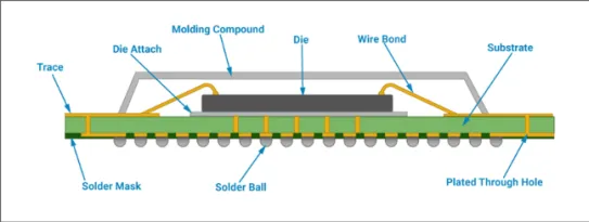 Packaging StructureIn addition to the traditional Wire Bonding BGA packaging method, the mainstream method currently is Flip Chip BGA, which allows for smaller packaging sizes by flipping the chip and connecting it to the substrate. This technology first forms metal bumps on the wafer die pads through wafer bumping processes, and then connects these bumps to the underlying substrate. Compared to the aforementioned methods, the significant differences between the two can be clearly seen. There are various types of chip packaging, which can be classified based on the materials used, mainly into plastic encapsulated chips, ceramic packaged chips, and metal packaged chips. Among these, ceramic and metal packaging materials are primarily used in extremely harsh working conditions such as aerospace and military applications, and the costs of these materials are relatively high. If classified by packaging structure, it becomes even more diverse, as different types of chips and application requirements necessitate different structural forms of packaging. Packaging StructureIn addition to the traditional Wire Bonding BGA packaging method, the mainstream method currently is Flip Chip BGA, which allows for smaller packaging sizes by flipping the chip and connecting it to the substrate. This technology first forms metal bumps on the wafer die pads through wafer bumping processes, and then connects these bumps to the underlying substrate. Compared to the aforementioned methods, the significant differences between the two can be clearly seen. There are various types of chip packaging, which can be classified based on the materials used, mainly into plastic encapsulated chips, ceramic packaged chips, and metal packaged chips. Among these, ceramic and metal packaging materials are primarily used in extremely harsh working conditions such as aerospace and military applications, and the costs of these materials are relatively high. If classified by packaging structure, it becomes even more diverse, as different types of chips and application requirements necessitate different structural forms of packaging.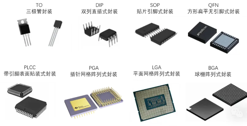 Illustration of Different Structural Types of Chip PackagingAs the market demand for high-performance chips continues to rise and the application fields of chips expand, packaging technology is also rapidly evolving. From the initial planar 2D packaging gradually moving towards 2.5D and even 3D packaging, the aim is to drive the continuous improvement of chip integration through technological innovation. Currently, the highly anticipated AI large chip, namely AI SoC (System-on-Chip), requires the integration and packaging of 2 to 8, or even more high-bandwidth HBM storage dies (collectively referred to as KGD, or Known Good Die) and thus places higher demands on packaging technology. To ensure high-speed and stable interconnect bandwidth between HBM storage dies and the main chip die, advanced CoWoS 2.5D packaging technology has emerged. Illustration of Different Structural Types of Chip PackagingAs the market demand for high-performance chips continues to rise and the application fields of chips expand, packaging technology is also rapidly evolving. From the initial planar 2D packaging gradually moving towards 2.5D and even 3D packaging, the aim is to drive the continuous improvement of chip integration through technological innovation. Currently, the highly anticipated AI large chip, namely AI SoC (System-on-Chip), requires the integration and packaging of 2 to 8, or even more high-bandwidth HBM storage dies (collectively referred to as KGD, or Known Good Die) and thus places higher demands on packaging technology. To ensure high-speed and stable interconnect bandwidth between HBM storage dies and the main chip die, advanced CoWoS 2.5D packaging technology has emerged.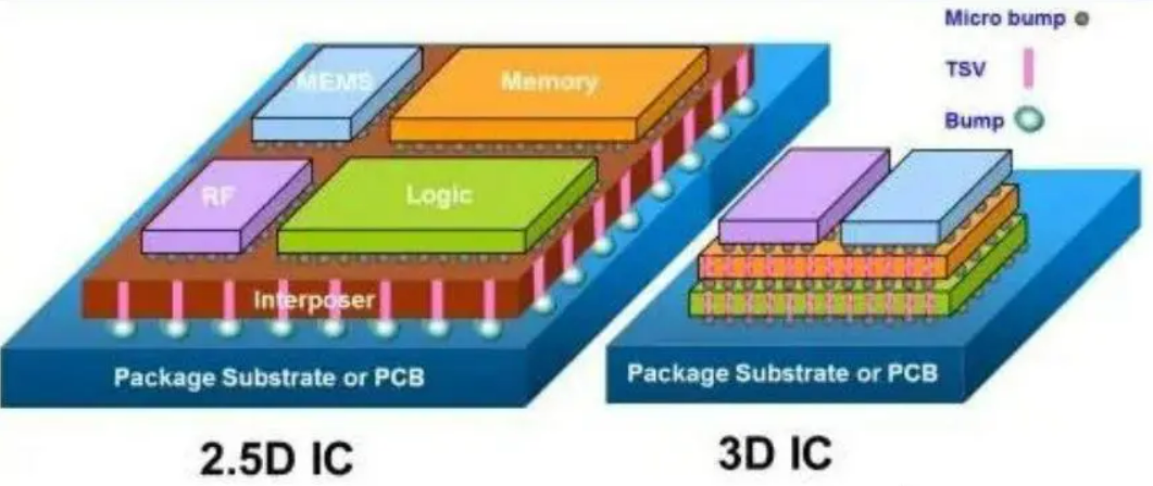 2.5D and 3D Packaging 2.5D and 3D Packaging
Final Test
Before the chips are officially shipped and delivered to end product customers, they must undergo a crucial testing phase—Final Test (FT)—to ensure their functionality and quality meet standards. The necessity of this step arises from two main reasons. First, while CP testing can effectively assess chip performance, it is limited by the power and frequency of the testing conducted at the wafer level through probing. Second, during the packaging process, chips may incur some degree of damage due to process factors. Therefore, conducting FT testing on the final packaged product is essential, as it effectively identifies and eliminates potential quality issues.FT testing is quite similar to CP testing in terms of testing methods, also relying on ATE automatic testing machine equipment. In addition, auxiliary tools such as load boards and handlers are required. These devices and tools work together to ensure the accuracy and efficiency of FT testing, providing solid quality assurance for the final shipment of the chips. FT Testing Process and Related Equipment FT Testing Process and Related Equipment
System Level Testing (SLT Test)
As chip sizes, functionalities, and packaging technologies continue to advance, their complexity also increases, leading to significant cost increases for CP and FT testing, along with limited testing coverage. This is especially true in certain special fields with extremely strict defect rate requirements for chips, such as autonomous driving chips, where the quality requirements for testing are even more stringent. To effectively reduce the shipment defect rate, known as DPPM (Defective Parts Per Million), many chips have added an additional SLT testing phase after completing FT testing.SLT testing is designed based on the actual application scenarios of the chips, aiming to simulate real chip business flows during the testing process through carefully crafted test boards and established testing procedures. This testing method aims to ensure that the chips have passed a more rigorous inspection that is closer to “real application scenarios” before being shipped to customers and applied to actual product boards, thereby reducing the DPPM defect rate to a lower level. This initiative not only improves chip quality but also enhances customer confidence in the products. The relationship between chip packaging and testing is closely intertwined, which is why typical manufacturers in the industry are often referred to as packaging and testing factories.Shenzhen Zhongke System Integration Technology Co., Ltd. was established in 2011 and has been deeply engaged in the advanced packaging field for over a decade, accumulating extensive experience in advanced packaging design simulation and process development. The company’s main business includes wafer-level packaging, IC test board design and processing, hardware design and development, and one-stop solutions for advanced packaging. In 2021, the company was wholly acquired by Chipright Micro (Shanghai) Electronics Technology Co., Ltd. and is now an excellent one-stop service provider for advanced system-level packaging design in China, with products widely used in aerospace, vehicles, ships, communications, electronics, and medical industries.Chip packaging and testing are crucial links in the semiconductor integrated circuit industry chain, essential for the physical shell protection, functional integrity, and performance reliability of integrated circuit chips.With the rapid advancement of technology, future packaging testing technologies will continue to move towards miniaturization, high density, and high integration, such as adopting cutting-edge processes like 3D packaging and wafer-level packaging.These innovative technologies enable chips to achieve more diverse functions and excellent performance in more compact spaces, thereby meeting the growing demand for chips in diverse application fields such as artificial intelligence, the Internet of Things, 5G communications, and automotive electronics. This not only drives the vigorous development of the semiconductor integrated circuit industry but also injects new vitality and opportunities into the entire technology industry.
|