1. The Relationship Between I²C Timing and AT24Cxx Driver
AT24Cxx (24C02/04/08/16…) is an EEPROM storage chip that communicates with the MCU via the I²C bus.The essence of I²C is:
Using two wires (SCL, SDA) to read and write data according to a fixed timing.
| Signal Line | Meaning |
|---|---|
| SCL | Clock line, controlled by the master (MCU) |
| SDA | Data line, where the data is transmitted |
I²C is a typical “timing protocol” that must adhere to strict rules such as start signal, stop signal, acknowledgment, and data validity.
2. Key I²C Timing Review
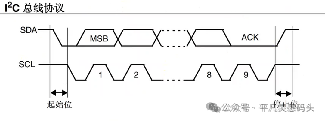
The core operations of I²C include:
-
Start Condition (START)
-
SCL = High
-
SDA transitions from high to low
Stop Condition (STOP)
-
SCL = High
-
SDA transitions from low to high
Acknowledgment (ACK)
-
The receiver pulls SDA low (0) to indicate ACK
-
Releasing SDA (1) indicates NACK
Data Transmission
-
SDA must remain stable when SCL = High
-
Data changes can only occur when SCL = Low
3. Detailed Explanation of Functions
1) IIC Start Signal:<span><span>iic_star()</span></span>
void iic_star(void){SCL_L; SDA_H; SCL_H;timer5_delay_us(5);SDA_L;timer5_delay_us(5);SCL_L;}Function Description
<span>iic_star()</span> is used to generate the I²C Start Signal (START).
The standard definition of the START condition is:
When SCL is high, SDA transitions from high to low.
This is the only legal way to start according to I²C specifications; all communication must begin with START.
Line-by-Line Analysis
① <span>SCL_L;</span>
-
Pull the clock line low first.
-
Why? Because only when SCL is low can SDA change levels without being interpreted as a START/STOP signal.This is understandable, right?
② <span>SDA_H;</span>
-
Pull SDA high first (ensuring it is in a stable “high to low” transition state)
-
This is to create the falling edge later.
③ <span>SCL_H;</span>
-
Now pull the clock line high.
-
This is the key preparation state for I²C START.
④ <span>SDA_L;</span> (The Main Event)
-
When SCL = High, let SDA transition from high to low
-
Complete the Start Signal (START)
⑤ <span>SCL_L;</span>
-
Immediately pull SCL low after the start signal is completed, so that subsequent data transmission can begin.
Summary
<span>iic_star()</span> generates the START condition strictly according to the I²C protocol.
The essence of the start signal: SDA generates a falling edge when SCL is high.
2) IIC Stop Signal:<span><span>iic_stop()</span></span>
Original Code
void iic_stop(void){SCL_L;SDA_H;SCL_H;timer5_delay_us(5);SDA_H;timer5_delay_us(5);}STOP Condition Definition:
When SCL is high, SDA transitions from low to high, which is STOP.
Line-by-Line Analysis:
-
Preparation: Pull SCL low, pull SDA high
-
SCL goes high → Preparing for STOP
-
SDA ensures transition from low to high → STOP is generated
STOP is the end signal of communication, and AT24Cxx will start its internal write cycle after STOP (during write operations).
For the following receive ACK/NACK signals and send ACK/NACK signals, remember this sentence
Receive ACK/NACK Signal
The master will send a bit of data on the next clock after receiving a byte, where data 0 indicates ACK and data 1 indicates NACK.
Send ACK/NACK Signal
The master will receive a bit of data on the next clock after sending a data byte, where data 0 indicates ACK and data 1 indicates NACK
3) Send ACK/NACK:<span><span>iic_send_ack(u8 ack)</span></span>
void iic_send_ack(u8 ack){SCL_L; timer5_delay_us(3); ack ? (SDA_H) : (SDA_L);timer5_delay_us(2);SCL_H; timer5_delay_us(5);SCL_L;}Concept Explanation
-
ACK = 0: Reception successful
-
NACK = 1: Indicates no need to continue receiving (usually used for the last byte)
Explanation
In I²C:
| ACK | SDA Level |
|---|---|
| 0 | Pulled low (valid acknowledgment) |
| 1 | Released to high (no acknowledgment) |
After the master sends a byte, it waits for the slave to acknowledge; after the master reads a byte, it must send ACK/NACK.
4) Read Slave ACK:<span><span>iic_get_ack()</span></span>
u8 iic_get_ack(void){ u8 ack;SCL_L; SDA_H;SCL_L; timer5_delay_us(5);SCL_H;timer5_delay_us(5);if(SDA_READ_INT) { ack = 1; }else { ack = 0; }SCL_L; return ack;}Explanation
-
Read whether the slave pulls SDA low.
-
The master must configure SDA as input (high impedance), so first
<span>SDA_H</span>. -
If SDA=0 → ACK
-
If SDA=1 → NACK
After writing to AT24Cxx, it will be in an internal busy state, and ACK will be crucial.
5) Send 1 Byte:<span><span>iic_send_byte()</span></span>
void iic_send_byte(u8 data){ u8 i;for(i=0;i<8;i++) { SCL_L; timer5_delay_us(3);if(data & 0x80) { SDA_H; }else { SDA_L; } timer5_delay_us(2); SCL_L; timer5_delay_us(5);data = data << 1; }SCL_L;}Explanation
The process complies with the basic rules of I²C:
Data bits must be stable before the rising edge of SCL and remain unchanged during the high period.
Loop 8 times, sending each bit of data from high to low.
6) Receive 1 Byte:<span><span>iic_read_byte()</span></span>
u8 iic_read_byte(void){ u8 i; u8 data;SCL_L; SDA_H;for(i=0;i<8;i++) { SCL_L; timer5_delay_us(5); SCL_H; timer5_delay_us(5); data = data << 1; if(SDA_READ_INT) { data |= 0x01; }}SCL_L; return data;}Explanation
-
SDA is set to input (high impedance)
-
The master reads SDA when SCL is high
-
Read 8 bits to form a byte
After reading, the master must send ACK or NACK (see previous functions).
In the next section, we will use the functions we encapsulated above to write the low-level driver for AT24C02.