First, a little aside~ It is said online that the IIC of STM32F103 has flaws! Let’s just consider it as some shortcomings; personally, I think it can definitely be used, but it is not easy to use. Because ST Company considered patent issues, they did not follow Philips’s standards. This leads to the IIC of STM32 being very complicated to use. Below, I will discuss the precautions for simulating IIC using STM32 IO ports:
IIC bus timing:
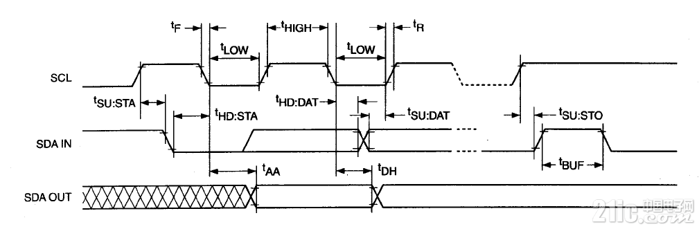
Getting to the main topic→_→ The author suffered losses due to not understanding the acknowledgment correctly. Let’s talk about several important states of IIC:
1. Idle State: When the IIC bus is idle, both the SDA and SCL lines are at a high level. Since the devices connected to the bus must be open-drain and collector open (as for why, readers can search for themselves), whenever any device outputs a low level at any time, it will cause the signals on the bus to go low, meaning the relationship between the SDA and SCL of each device is logical AND. Because the output ends of each device are open-drain, they must be connected to the power supply through pull-up resistors to ensure that SDA and SCL are pulled high when idle.
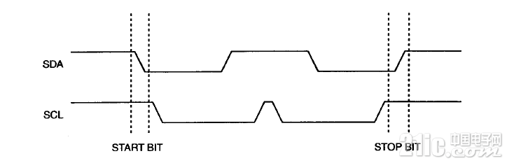
2. Start Signal S and Stop Signal P (Note the timing in the start and stop signals, strictly follow the data manual; being a bit fast or slow is not acceptable!):
Start Signal S: The change of the SDA line from high to low during the high level of the SCL line indicates the start signal, and only after the start signal are other commands valid.
Stop Signal P: The change of the SDA line from low to high during the high level of the SCL line indicates the stop signal. With the appearance of the stop signal, all external operations are concluded. As shown:
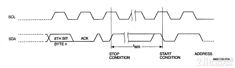
3. Data Transmission: In short: low level changes, high level stable.
During data transmission on the IIC bus, each data bit’s transmission corresponds to a clock pulse. During the high level of the clock pulse, the data on the data line must remain stable; changes in the data line’s level are only allowed during the low level of the clock line. That is: the data must be prepared before the rising edge of SCL and must be stable before the falling edge. As shown:
4. (Common Mistake) Acknowledgment Signal ACK, Non-Acknowledgment Signal NACK, Stop Signal P:
Acknowledgment Signal ACK: This signal is generated by the slave device. The IIC bus must have an acknowledgment signal A after transmitting one byte (8 bits) of data. The common mistake here is that the requirement for a valid acknowledgment bit ACK is that the receiver must pull the SDA line low during the low level before the ninth clock pulse and ensure it is stable low during the high level of that clock. This indicates that it has received an 8-bit data. As shown:
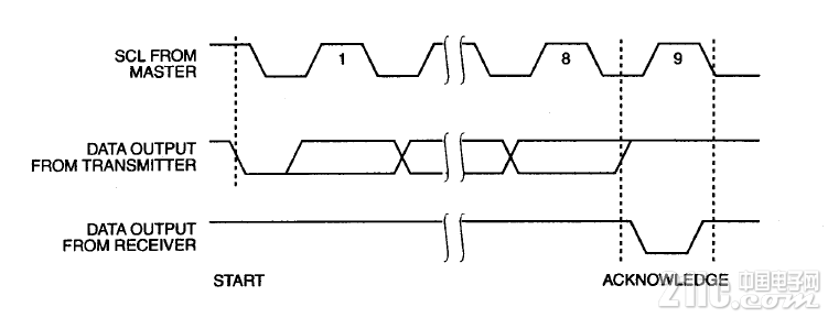
Non-Acknowledgment Signal NACK: This signal is generated by the master device. When the master device receives data from the slave, after receiving the last data byte, it must send a non-acknowledgment signal to the slave device, allowing the slave to release the data bus so that the master can send a stop signal, thus ending the data transmission.
Stop Signal P: The master sends a stop signal in two cases: 1. After data transmission is complete, the master device sends a stop signal. 2. For some reason, if the receiver does not respond to the master device’s addressing signal, for example, if the receiver is busy with other processing and cannot receive data on the bus, it must release the bus and pull the data line high, while the master device generates a stop signal to end the data transmission on the bus.
From the above, we can see:
1. Regardless of the data transmission format (master sends, slave receives; master receives, slave sends; master both receives and sends), the addressing byte is sent by the master device, and the direction of data transmission is determined by the direction in the addressing byte.
2. The addressing byte only indicates the address of the slave device and the direction of data transmission. Among the n data addresses inside the device, the device designer specifies the first data byte as the internal unit address pointer in the IIC bus data operation format of that device and sets the address auto-increment function to reduce the addressing operations of the slave device.
3. Each byte transmission must have an accompanying acknowledgment signal.
4. The slave device must release the data bus to a high level after receiving the start signal (last image), so that the master device can send the slave address.
Author: Houqi