In the process of PCB manufacturing and soldering, the issue of solder balls or solder ball blockage in solder mask vias is a common yet troublesome problem. Solder balls not only affect the aesthetic quality of the product but can also lead to circuit shorts, severely impacting the reliability and lifespan of the product. Today, we will delve into this issue.
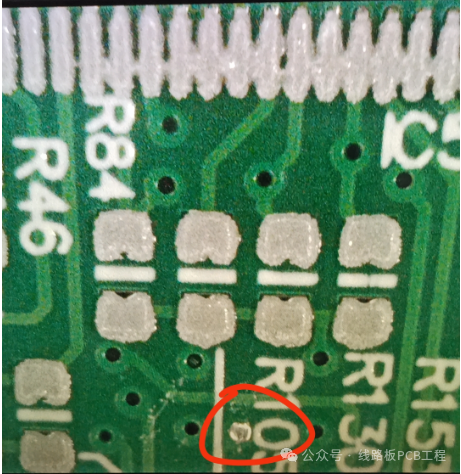
1. Root Cause Analysis
The solder ball blockage issue primarily occurs during the reflow soldering process. When the PCB is subjected to high-temperature soldering, residues of flux or moisture within the vias evaporate due to heat, forcing the molten solder out of the vias and forming solder balls. This situation is more likely to occur under the following conditions:
1. Unreasonable via design dimensions
2. Improper solder mask treatment process
3. Inaccurate control of soldering temperature
2. Solutions
1. Via Size Design
The design of via diameter is crucial. Oversized vias increase the space for solder filling, making it easy to accumulate excess solder; undersized vias may prevent the solder mask material from fully covering. It is recommended to follow these design principles: control the via diameter between 0.2-0.4mm.
Maintain sufficient spacing between vias to avoid overlapping thermal effects during soldering.
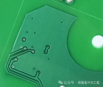
2. Aluminum Plugging Process
The aluminum plugging process is currently one of the most effective solutions, but it requires strict control of process quality:
Material selection for plugging: Use specialized aluminum plugging materials to ensure their thermal expansion coefficient matches that of the PCB substrate.
Key points for process control:
The depth of the plugging must be uniform to avoid voids or unfilled areas.
The curing temperature and time must be precisely controlled to ensure complete curing of the material.
The surface flatness must meet requirements to avoid affecting subsequent soldering.
3. In addition to the two main directions mentioned above:
Selection of solder mask ink: Use solder mask ink with moderate viscosity and good fluidity.
Pre-baking treatment: Properly bake the PCB before soldering to remove moisture.
Optimization of soldering parameters: Adjust the reflow soldering temperature curve to avoid abrupt temperature changes.