1 Abstract
With the continuous development of new energy technologies and the increasing awareness of green and low-carbon living, the energy sector is accelerating its transition to clean and low-carbon solutions. The diversification of energy storage modes and technologies is crucial, as energy storage is an important technology and foundational equipment supporting new power systems. New energy generation is characterized by randomness and intermittency, with diverse power supply forms and energy flow directions. Traditional power equipment struggles to meet the diverse and complex requirements of power control, leading to the widespread application of distributed energy generation and matching energy storage devices. Energy storage battery units are key components of energy bus systems, and their battery management systems hold significant research significance and application value.
This paper focuses on the battery management system, examining aspects such as system topology, basic principles, and control strategies. It specifically addresses battery management, charge and discharge control technologies, and the estimation of the battery state of charge (SOC). The specific content includes: determining the energy bus topology through the study of the energy bus system structure, analyzing the system’s operational modes to research control methods for achieving voltage regulation and power control of bidirectional DC-DC converters; conducting experiments and parameter identification on batteries for easy management and charge/discharge control; and estimating the battery SOC using the extended Kalman filter method. A simulation model of the energy bus topology was constructed, and the simulation results indicate that the energy bus topology operates stably. For the converter control method, a converter circuit simulation model was built in MATLAB/SIMULINK, and the simulation results show that the converter control method effectively achieves the preset control objectives with good steady-state and dynamic performance. Based on experimental data, an extended Kalman filter SOC estimation model was established, yielding high-precision estimation results that meet design requirements. The specific implementation of the hardware and software for the experimental prototype was designed.
An experimental prototype was built, completing charging and discharging experiments on the battery, and testing the operating waveforms of the DC-DC converter. The experimental results generally meet design requirements, and the converter operates in a soft-switching state. The above experimental results validate the stability and feasibility of the designed energy bus battery management system, which, along with the DC-DC converter, can be applied to energy bus systems.
2 Research on Energy Bus Topology
This paper designs a battery management system for the energy bus, which connects energy storage battery units, photovoltaic generation units, and load units. It analyzes the basic topology of energy routers in typical energy bus structures. Focusing on the topology, main operational modes, and performance indicators of the energy bus system, this research lays the foundation for subsequent battery management system design through operational simulation experiments of the energy bus system structure.
2.1 Energy Bus Battery Balancing
2.1.1 Basic Structure of Energy Bus Type Battery Balancing
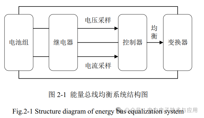
The energy bus type battery balancing system structure maximizes energy utilization through energy conversion and transmission within the system. In this system structure, high remaining charge batteries charge low charge batteries through energy bus conversion. During system operation, the energy bus is responsible for energy transmission, while the system microprocessor gates the energy bus, hence this energy channel is referred to as the energy bus. The system structure diagram is shown in Figure 2-1.
 The main functions of this system are:
1) A relay is connected in parallel on the battery side, serving as a switch to open battery detection information and a switch to enable energy transfer from the battery with the maximum remaining charge;
2) The voltage and current sampling module is responsible for collecting the voltage and current information of the battery;
3) An energy transmission module composed of an inverter and transformer, used for energy transmission and voltage transformation of the battery;
4) The rectification and filtering unit rectifies and filters the voltage output from the transformer for charging. The main steps to achieve balancing in this system structure are: First, the system is activated, and the battery status information, such as voltage and current, is detected and transmitted to the microprocessor; Second, based on the detected battery status information, the SOC of the battery is estimated; Third, the need for balancing is determined based on the battery SOC value; if balancing is not needed, it will not proceed until the balancing conditions are met; Fourth, when the balancing conditions are satisfied, the time required for balancing is calculated based on the difference in SOC values between the batteries; Fifth, balancing is initiated, transferring energy from high charge batteries to low charge batteries through the energy bus, and once the transfer time is completed, the energy transmission is closed, completing the battery balancing.
2.1.2 Energy Bus Type Low Power Balancing Structure
As shown in Figure 2-2, this is a balancing circuit structure applied in low power scenarios, where only two battery groups are analyzed for basic principles, represented as Cell1 and Cell2. In actual design, the circuit can be increased or decreased according to the number of batteries based on actual needs, allowing for complex applications. The balancing signal from the controller achieves battery group balancing. Capacitors and resistors are used to isolate the circuit while also driving the MOSFETs in the circuit, with the control signals for the MOSFETs varying based on the circuit structure, effectively simplifying the MOSFET driving circuit.
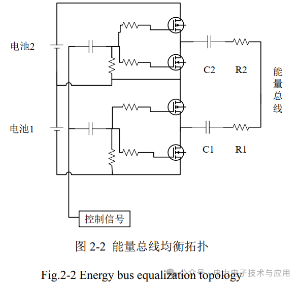 As shown in Figures 2-3 and 2-4 , these are two different operating states of the energy bus balancing topology shown in Figure 2-2. Figure 2-3 shows the MOSFET in the conducting state when the control signal is high, while Figure 2-4 shows the MOSFET in the off state when the control signal is low.
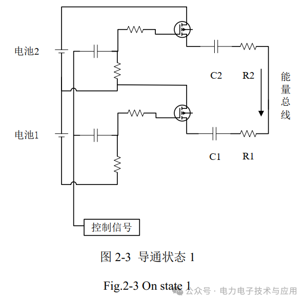 Figure 2-3 shows the conducting state of the MOSFET when the control signal is high, connecting the positive terminals of the two batteries, with the voltage corresponding to the battery voltage. However, the voltage of the capacitor connected to the energy bus does not change abruptly; the high voltage capacitor transfers energy to the low voltage capacitor, with the current being transferred from the high voltage battery to the low voltage battery.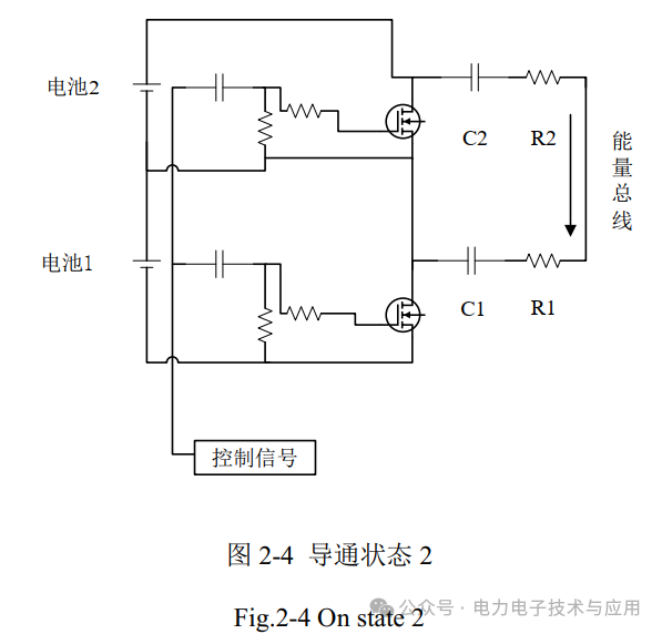
Figure 2-4 shows the MOSFET in the off state when the control signal is low, connecting the negative terminals of the two batteries, with the voltage corresponding to the battery voltage. Similarly to Figure 2-3, the voltage of the capacitor connected to the energy bus does not change abruptly; the high voltage capacitor transfers energy to the low voltage capacitor, with the current being transferred from the high voltage battery to the low voltage battery.
2.1.3 High Power Switch Mode Power Supply Balancing Circuit Structure of Energy Bus
The high power balancing circuit is also based on the energy bus, utilizing a DC-DC converter to achieve energy transmission, enhancing balancing speed and flexibility. The design of the DC-DC converter in the high power energy bus balancing circuit primarily meets the power requirements of system operation.
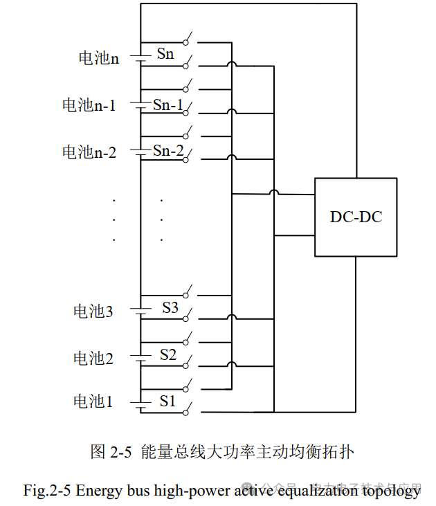
As shown in Figure 2-5, this is a high power balancing topology that can connect multiple battery cells, with each battery equipped with a switch, and using a DC-DC converter to connect the energy bus and the battery. Energy transmission occurs through the energy bus, which also detects the battery status information, allowing energy from the energy bus to be transferred to batteries with low charge.
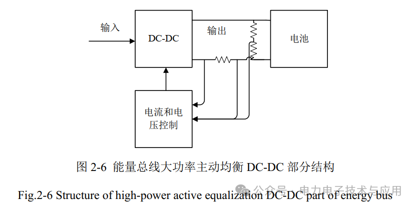
 In the above energy bus topology, the DC-DC converter needs to be designed separately to ensure that the output voltage and circuit characteristics of the DC-DC converter match the voltage and current characteristics of the battery, preventing overcharging and overvoltage, thus ensuring stable system operation. As shown in Figure 2-6, this is the structural part of the DC-DC converter in the energy bus topology.
 Due to space limitations, the following sections are omitted. For the original text, please contact [email protected]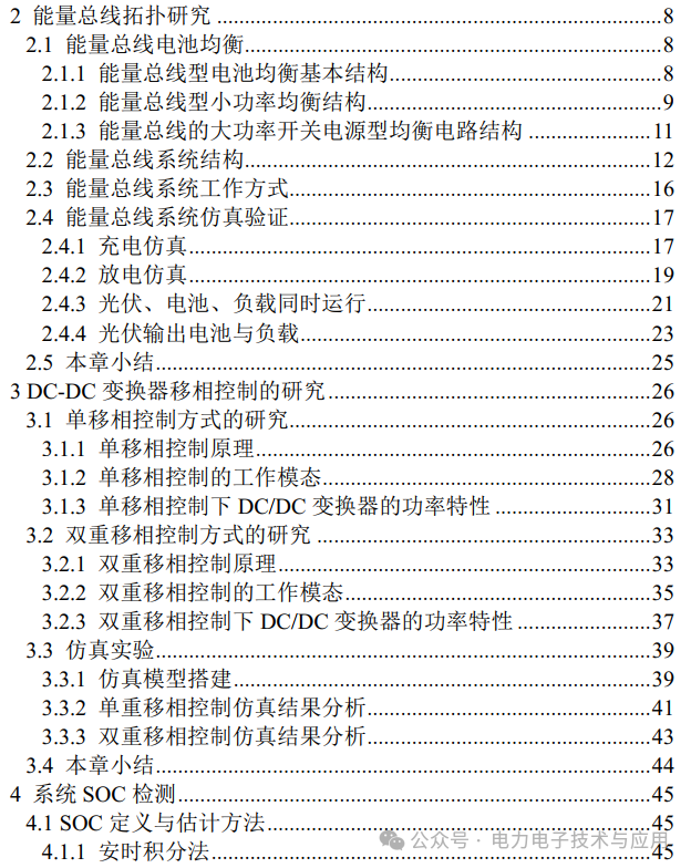

5.4 Hardware Circuit Design
5.4.1 DC-DC Main Circuit
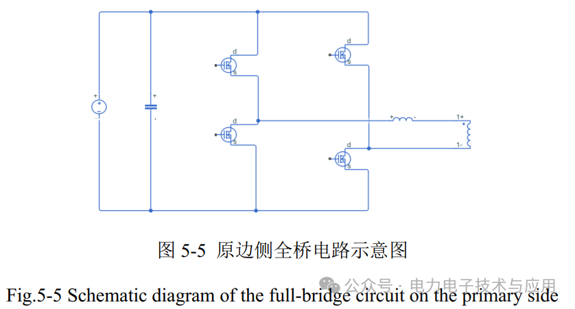
The schematic diagram of the full-bridge main circuit on the primary side is shown in Figure 5-5. Based on the parameter calculations and component selection mentioned above, the components on the primary side need to have a high voltage rating. Among them, three series-connected horn-type electrolytic capacitors with a rated voltage of 450V and a tolerance of ±20%, 680µF, ensure that the capacitor’s voltage rating and capacity meet design requirements. The driving signal for the switching tube is provided by the driving circuit and connected to it, which will be detailed in the design of the driving circuit below. The total capacitance of the series capacitors results in an input electrolytic capacitor capacity of approximately 227uF.
The schematic diagram of the full-bridge circuit on the secondary side is shown in Figure 5-6. According to the converter selection parameters, the full-bridge main circuit on the secondary side must withstand large currents, so thicker traces must be provided during PCB fabrication, using copper bars to increase the current-carrying capacity and prevent damage to the converter.
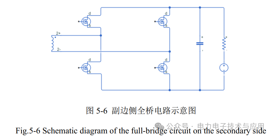 Among them, the capacitor is selected with a rated voltage of 200V, a capacitance value of 1000µF, and a tolerance of ±20%, with two series-connected horn-type electrolytic capacitors ensuring that the capacitor’s voltage rating and capacity meet design requirements. The total capacitance of the series capacitors results in an output electrolytic capacitor capacity of 500µF. The driving signal for the switching tube is provided by the driving circuit and connected to it.5.4.2 Driving Circuit
Since the STM32 chip cannot output the gate voltage level for the MOSFET, a separate driving circuit is required for the switching tube, which needs to be designed. The driving circuit amplifies the driving signal to drive the switching tube and isolates it from the power circuit. As shown in Figure 5-7, this design uses the NSI-6602B driving chip, which can simultaneously drive two switching tubes. The driving circuit must meet the following requirements: First, it must provide sufficient gate voltage during the conduction of the power switching device and maintain it during conduction; Second, it must provide stable driving current to ensure the rapid conduction of the switching tube; Third, it must provide reverse bias voltage to ensure the switching tube turns off; Fourth, it must ensure electrical isolation between the control circuit and the power circuit to prevent interference from the power circuit to the control circuit.
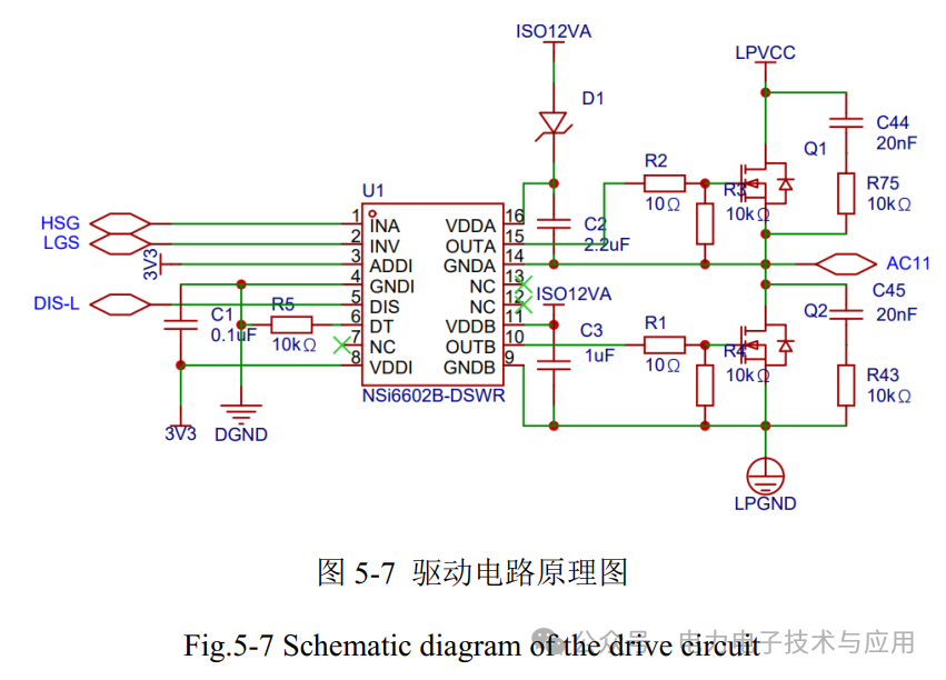
In addition, the bidirectional full-bridge DC-DC converter driving module belongs to a low power circuit, so it is necessary to consider the interference of the power circuit on the driving circuit and other weak signal circuits. The layout should consider: First, small signals should be kept away from the power circuit bus to avoid interference from parallel buses; Second, during layout, small signal circuits should be concentrated, and power circuits should be concentrated, improving anti-interference capability through separation and reduced area; Third, the loop area should be minimized, and wiring distance should be shortened; Fourth, digital signal and analog signal circuits should be separated, and digital ground and analog ground should be divided; Fifth, the wiring connecting the digital ground plane and the analog ground plane should be thickened to enhance anti-interference capability. Following these layout and wiring rules, copper should be laid on the bottom layer, distinguishing between analog ground and digital ground, and connected through 0Ω resistors to achieve good anti-interference capability.
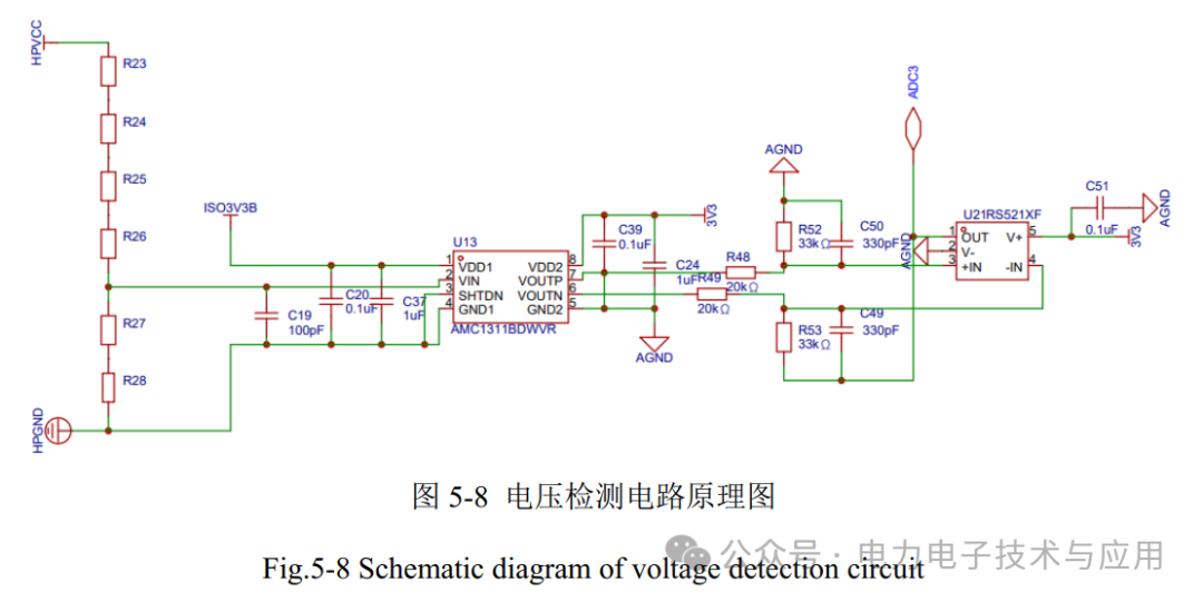
5.4.3 Voltage Detection Circuit
In this design system, it is necessary to detect the voltage on the primary side and the secondary side, i.e., the battery voltage. The voltage signal is a strong electrical signal greater than 3.3V from the power circuit, which cannot be read directly by the microcontroller. A Hall sensor or resistor divider method can be used to convert it into a low power weak signal. This design uses a high-precision resistor divider, and the circuit schematic is shown in Figure 5-8. Since the voltages on the primary and secondary sides of the converter differ, resistors of different values should be selected reasonably, preferably with higher precision. The primary side is calculated for a maximum of 400V, and the secondary side for a maximum of 80V, requiring an output voltage of 0-3.3V, which is then amplified through the isolation amplifier AMC1311BDWVR and filtered before being input to the microcontroller’s AD module.
5.4.4 Current Detection Circuit
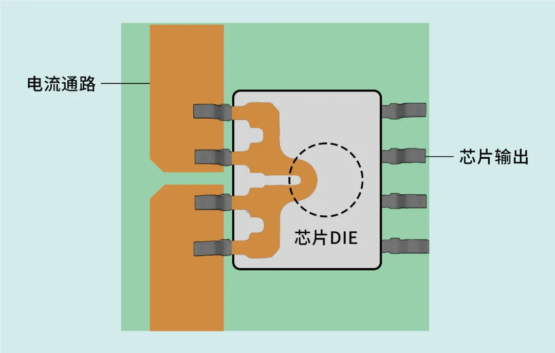
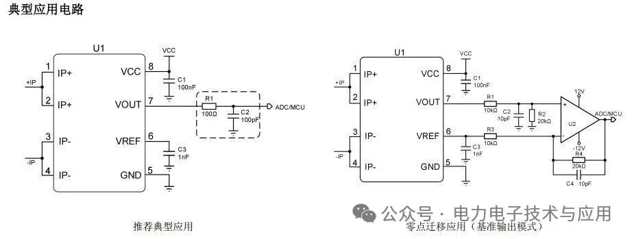
In this design system, it is necessary to detect the current on the primary side and the secondary side, specifically the charging and discharging current of the battery. The CC6902B series high-performance Hall effect current sensor from Chengdu Xinjing Electronics is used, which outputs a voltage between 0.33-2.97V linearly varying with the magnetic field under a power supply voltage of 3.3V, with a linearity of up to 0.1%. In the absence of current, the static output is 50%VDC. As shown in Figure 5-9, the current detection circuit schematic shows that after the Hall sensor is connected to the main circuit, the current signal is filtered and amplified before being transmitted to the microcontroller’s AD module.
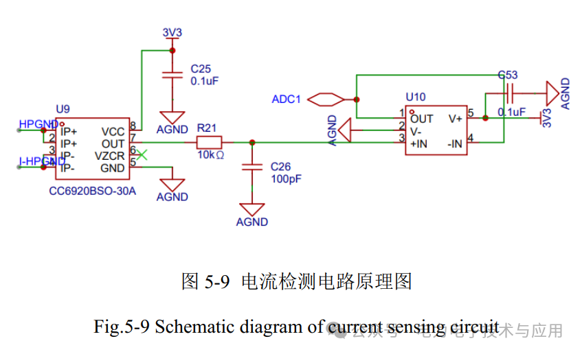
CC6902 is a high-performance single-ended output linear current sensor produced by Chengdu Xinjing Electronics, which can effectively detect AC or DC current, widely used in industrial, consumer, and communication devices.
It has now been upgraded to CC6937, which is a domestically produced high-performance Hall effect current sensor that can more effectively measure DC or AC current, with advantages such as high accuracy, good linearity, and temperature stability, widely used in industrial, consumer, and communication devices.
Features
-
Reference has built-in VREF output and external VREF input modes:
-
When using built-in VREF output, VOE can be programmed to <5mV
-
When using external VREF input, the static output voltage of VOUT remains consistent
-
Wide measurement range, with multiple ranges available: 5A, 10A, 20A, 25A, 30A, 40A, 50A, 60A
-
High isolation voltage, with a safety isolation voltage of 3750VRMS from the lead pins to the signal pins
-
High bandwidth (230kHz), low noise, single-ended analog output
-
Low loss, with a lead resistance of 0.5mΩ
-
Step response time of 1.5us
-
Temperature error of ±1%, with sensitivity temperature drift of up to ±2.5%
-
Good temperature stability, using Hall signal amplification and temperature compensation circuits
-
Differential Hall structure, strong resistance to external magnetic interference
-
ESD (HBM) 4kV, ESD (CDM) 1kV, LU 200mA
5.4.5 Protection Circuit
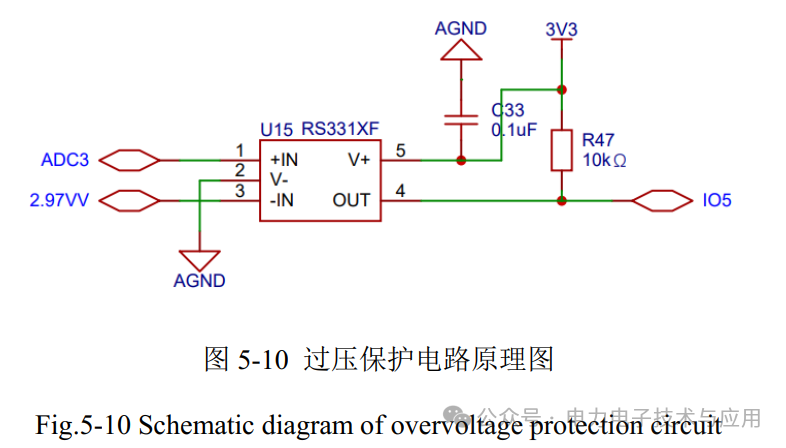
In this design, after the microcontroller detects the voltage and current information as described above, the schematic diagram of the overvoltage protection circuit is shown in Figure 5-10. The comparator RS331XK compares the voltage information transmitted through the ADC4 pin with a reference voltage of 2.475V. If it exceeds this value, it indicates that the voltage of the converter’s main circuit exceeds the set value, with 2.475V corresponding to 300V on the primary side.
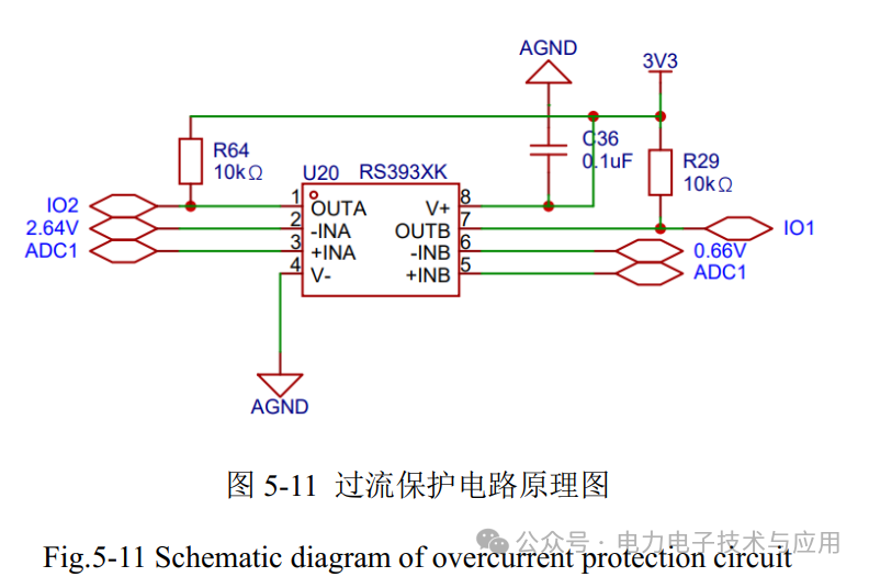
As shown in Figure 5-11, this is the schematic diagram of the overcurrent protection circuit. The comparator RS393XF compares the current information transmitted through the ADC1 pin with a reference voltage of 2.64V. If it exceeds this value, it indicates that the primary side current of the converter’s main circuit reaches 60% of the sensor’s full scale; similarly, if it is less than 0.66V, it indicates that the reverse current of the primary side exceeds 60% of the sensor’s full scale. This value is determined by the maximum current on the primary side, as defined by the main circuit design parameters, and the sensor range, with redundancy considered to ensure that actual operation remains within a safe and stable range, preventing damage to the converter’s main circuit.
 5.4.6 Power Supply Circuit
The stability of the power supply circuit is crucial for the normal operation of all chips in the system. The schematic diagram of the power supply circuit is shown in Figures 5-12, 5-13, and 5-14. In this design system, three power supplies are required: an external power input generating VDC12V, and VDC3.3V for powering other chips.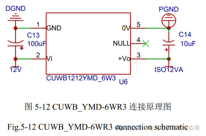 Considering that the converter requires four driving chips, i.e., four driving signals, which consume a significant amount of power, the DC/DC power module CUWB_YMD-6WR3 from Jinshengyang Company is used to generate isolated VDC12V, with isolated 12V voltage supplying both sides of the converter to ensure that the main converter is an isolated DC-DC converter. As shown in Figure 5-12, this is the connection schematic.
Due to space limitations, this paper only presents part of the content.
For the original text, please contact [email protected]
This article is a compilation of content from the internet, and the author expresses gratitude to the original authors. If there are any infringements, please contact the author for removal.
For more information on power electronics, please follow our public account.
<img src=”https://mmbiz.qpic.cn/mmbiz_jpg/SwFULVVNhkZ0kg2I6Yo2Tibbh2M2dlAV3dfH3CmXaNKlr3O2rCzoJicTzqzK22szibJAOjwIcSA93p605URKxAkoQ/640?wx_fmt=jpeg&wxfrom=5&wx_lazy=1&tp=webp#imgIndex=11″