After several days of effort, we have basically achieved the above requirements in this design, and proposed improvements in some functional aspects to make the system design more complete. In this design, we use an FPGA as the main controller, but due to time and equipment constraints, this design also has shortcomings, such as the measurement range cannot meet higher requirements, and there is significant room for improvement in measurement accuracy. We will continue to address these shortcomings and improve the measurement system design in our future studies.
1. Overall Design Scheme
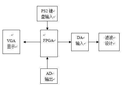
1.1 Main Control Module
Plan One: Use a microcontroller. Microcontrollers are widely used, but their processing frequency does not meet our requirements. Therefore, we can only use a processor with a faster processing speed.
Plan Two: Use Xilinx’s FPGA to implement the main controller. The internal IP core of Xilinx’s FPGA can easily generate DDS waveforms, which allows us to better generate the desired waveforms.
So we adopt Plan Two.
1.2 Display Module
Plan One: Use a TFT touchscreen. Color screens have the obvious advantages of low power consumption, small size, ultra-thin and lightweight, large information display, beautiful text, and comfortable vision. However, for FPGA, the control of the touchscreen cannot meet the control requirements well.
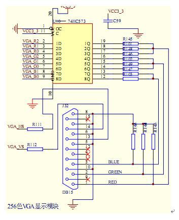
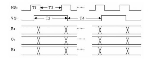
Plan Two: Use VGA display. FPGA can achieve control over VGA. VGA is widely used and the price is within an acceptable range. Moreover, for FPGA, controlling the VGA interface is more convenient and faster than controlling other displays, which saves us design trouble.
So we adopt Plan Two.
1.3 Input Module
Plan One: Use a matrix keyboard. The encoding of matrix keyboards is relatively simple and can achieve relatively complex control. However, the number of keys on a matrix keyboard is too few to allow for more data input.
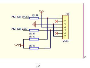
Plan Two: Use a PS2 keyboard. The control of the PS2 keyboard is simpler, and we can read data through two data lines, and the design of the PS2 keyboard better meets our design requirements, which determines the advantage of PS2 in this design.
Thus, we adopt Plan Two.
1.4 AD Output Module
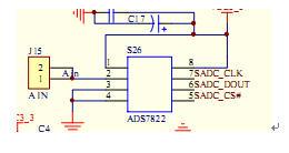
ADS7822 is a single-chip high-speed 12-bit successive approximation A/D converter. The ADS7822 has a bipolar circuit that forms a hybrid integrated conversion chip, characterized by fewer external components, low power consumption, and high precision, and it also has automatic zero calibration and automatic polarity switching functions, requiring only a few external resistive and capacitive components to form a complete A/D converter. Therefore, this plan adopts ADS7822 as the AD input component.
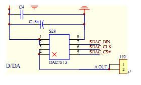
1.5 DA Output Module
DAC7513 is an 8-bit resolution D/A conversion integrated chip. It is fully compatible with microprocessors. This DA chip is widely used in microcontroller application systems due to its low cost, simple interface, and easy conversion control. The D/A converter consists of an 8-bit input latch, an 8-bit DAC register, an 8-bit D/A conversion circuit, and conversion control circuit.
2. Program Design
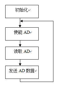
2.1 AD Output
–**********************Frequency Division Process*************************
process(clk)variable cnt1 : integer range 0 to 100;
variable cnt2 : integer range 0 to 20;
begin
if clk’event and clk=’1′ then
if cnt1=100 then
cnt1:=0;
if cnt2=20 then
cnt2:=0;
clock<=not clock;
if(cnt=3)then
cnt<=0;
else
cnt<=cnt+1;
end if;
else
cnt2:=cnt2+1;
end if;
else
cnt1:=cnt1+1;
end if;
end if;
end process;
–**************State Driven Process**********************
sync :process(clock,reset)begin
if(reset = ‘0’) then
current_state <= start;
elsif(clock’event and clock=’1′) then
current_state <= next_state;
end if;
end process sync;
–***************ADC Driver Process*******************
comb :process(current_state, intr)begin
case current_state is
when start => –Start State
next_state <= convert;
cs <= ‘0’;
wr <= ‘0’;
rd <= ‘1’;
read_data <= ‘0’;
when convert =>–Initialization
if(intr = ‘0’) then
next_state <= read1;
else
next_state <= convert;
end if;
cs <= ‘1’;
wr <= ‘1’;
rd <= ‘1’;
read_data <= ‘0’;
when read1 =>–Read State 1
next_state <= read2;
cs <= ‘0’;
wr <= ‘1’;
rd <= ‘0’;
read_data <= ‘1’;
when read2 =>–Read State 2
next_state <= start;
cs <= ‘1’;
wr <= ‘1’;
rd <= ‘1’;
read_data <= ‘0’;
when others =>–Other States
next_state <= start;
end case;
end process comb;
–****************Read AD Data********************
get_data: process(clock,reset)begin
if(reset = ‘0’) then
p<=0;
elsif(clock’event and clock=’1′) then
if(read_data = ‘1’) then
p<=conv_integer(data_i);
end if;
end if;
end process;
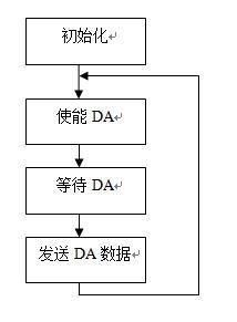
2.2 DA Output
–*********************65536Hz Frequency Division Process************************
process(clk)variable cnt1 : integer range 0 to 762;
begin
if clk’event and clk=’1′ then
case cnt1 IS
WHEN 381 =>
cp_65k<=’1′;
cnt1:=cnt1+1;
WHEN 762=>
cnt1:=0;
cp_65k<=’0′;
cp_wr<=’0′;
WHEN 20=>
cp_wr<=’1′;
cnt1:=cnt1+1;
WHEN OTHERS=>
cnt1:=cnt1+1;
end case;
end if;
end process;
–*********************1kHz Frequency Division Process************************
process(cp_65k)variable cnt1 : integer range 0 to 64;
begin
if cp_65k’event and cp_65k=’1′ then
case cnt1 is
when 32=>cp_1k<=’1′;
cnt1:=cnt1+1;
when 64=>cnt1:=0;
cp_1k<=’0′;
when others=>cnt1:=cnt1+1;
end case;
end if;
end process;
–**************DDS Address Accumulator Process**********************
PROCESS(cp_65k)BEGIN
IF(cp_65k’EVENT AND cp_65k=’1′) THEN
–DDS Accumulator Loop Adding dds_m
IF dds_add<65535 THEN
dds_add<=dds_add+dds_m;
ELSE
dds_add<=dds_add+dds_m-65536;
END IF;
END IF;
END PROCESS;
–***********************Frequency Increment/Decrement Control Process***************************
process(cp_1k)VARIABLE keys:INTEGER RANGE 0 TO 127 :=0; –Debounce Accumulator
begin
if cp_1k=’1′ then
case key is
when “10”=> –Frequency Increase
if keys=127 then
keys:=0;
bell<=’1′;
if dds_m=1000 then
dds_m<=1;
else
dds_m<=dds_m+1;
end if;
else
keys:=keys+1;
end if;
when “01”=> –Frequency Decrease
if keys=127 then
keys:=0;
bell<=’1′;
if dds_m=1000 then
dds_m<=1;
else
dds_m<=dds_m-1;
end if;
else
keys:=keys+1;
end if;
when others=>bell<=’0′;
end case;
end if;
end process;
end dac;
2.3 VGA Display
3. Performance Indicators
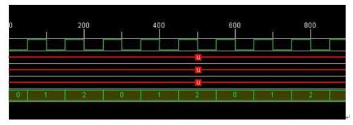
The waveform of the DA output
4. Summary
After several days of effort, we have basically achieved the above requirements in this design, and proposed improvements in some functional aspects to make the system design more complete. In this design, we use an FPGA as the main controller, but due to time and equipment constraints, this design also has shortcomings, such as the measurement range cannot meet higher requirements, and there is significant room for improvement in measurement accuracy. We will continue to address these shortcomings and improve the measurement system design in our future studies.
**********************************************
How to Share to Moments
Click the button in the upper right corner  →
→  Share to Moments
How to Follow “Changxue Electronics Network”
1. Enter WeChat “Contacts” → Click the upper right corner “Add” → Search for the public account “Changxue Electronics Network”
2. Or search for WeChat ID “Changxue Electronics Network”
3. You can also scan the QR code to follow:

**********************************************
Friendly Reminder:
Changxue Electronics Network Service Account: Changxue Electronics
Changxue Electronics Network Subscription Account: Changxue Electronics Network
**********************************************
www.eeskill.com Learn more exciting content!