1. Determine the Scheme and Purpose
Hello everyone, today I will introduce the LHA7668 chip from the F4 series development board, which is a domestic, 24-bit, 8-channel differential, and 16-channel single-ended high-precision low-power ADC chip.
The goal is to design a circuit board to meet the requirements for 16-channel single-ended acquisition or 8-channel differential acquisition.The specific content requirements are as follows:
[Basic Knowledge] Study notes on the 24-bit ADC eight-channel LHA7668 chip manual
01. Study the use of the LHA7668 chip and the development evaluation board;02. Design the first version of the PCB circuit board hardware;03. Version upgrades and optimization direction plans; Keywords: Linghuixichip, LHA7668 chip, LabVIEW, PCB design, analog signal acquisition. Note: High-definition images can be viewed via WeChat on mobile. 2. Trial Demonstration VideoAcquisition Target:2 different models of photodiodes and 6 different colored LEDs;Experimental Variable: Slowly changing light input;Acquisition Configuration: 24-bit ADC, eight channels, differential input, polling period of 0.8 seconds3. Introduction to Domestic LHA7668
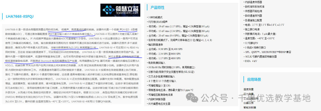
01. The LHA7668 domestic chip is a 24-bit high-precision, low-power, low-noise, highly integrated analog front-end chip.
02. The LHA7668 series pin is compatible with the AD7124 series, with a maximum rate of 38.4kHz in single-channel mode;
03. Under the trend of domestic substitution, it has certain competitiveness due to its performance advantages and domestic background;
04. From the application fields compatible with the AD7124 chip abroad, there is a large demand in industries such as industrial and medical;
05. In scenarios such as temperature/pressure/flow/optical, high precision and multi-channel have advantages.
06. In medical diagnostic equipment, the LHA7668 chip performs high-precision acquisition and conversion of biological electrical signals, such as multi-channel EEG, EMG, ECG monitoring devices, and blood pressure monitoring devices, which also have potential application prospects and help improve the accuracy of medical diagnosis.
07. The control of the LHA7668 chip is through a four-wire SPI bus, and the small package design makes it easier to integrate;01. Sensor Materials: Solar panels (photovoltaic panels), photodiodes (silicon batteries), yellow, red, blue, green, and white LEDs;Optical testing of LED photoelectric effects02. Purpose: The LEDs we commonly use also exhibit slight photoelectric effects; this experiment aims to verify the optical sensitivity of different photoelectric devices;03. Channels 2, 3, 4, 6, 7, and 8 are different colored LEDs, directly connected to the differential channels;04. Channel 1 is the solar panel, and SMA interface channel 5 is a photodiode commonly used in medical testing instruments;05. There is also a logic analyzer module on the left side to capture the timing sequence of the SPI bus, transplanting program testing functions;4. First Version of PCB Design
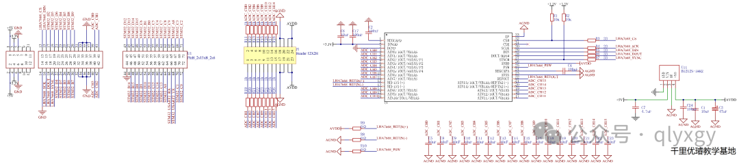
 01. The AVDD of the LHA7668 chip adopts a DCDC isolation design, U11 is the DCDC device, reducing power frequency interference;02. The AGND of the LHA7668 chip adopts a floating ground design, isolated from the power ground;03. Risk Point: The SPI bus does not adopt a fully isolated design, which may not achieve complete floating ground effect;04. Preliminary Correction Plan: Increase the SPI isolation scheme; since the signal lines are unidirectional, opto-isolation can be used, or the ISO154x series digital isolator chip scheme can be adopted;05. The reference design of [Linghuixichip] provides a 2.5V reference design, allowing for single-ended acquisition of other ranges using related operational amplifiers;06. The reference voltage of this circuit board is directly through the 5V reference after DCDC voltage regulation; the risk point is that the power quality of the DCDC regulator device does not meet standards, and the backup plan is to replace it with a high-quality imported DCDC device;07. The circuit board design reserves 0R resistors and signal test points for convenient debugging and adjustments of the experimental machine version;08. In the circuit board processing, SMT needs to meet the minimum mounting requirement of 70×70; the single board size is 45*59.5, so the design is a 2×1 array after 90*59.5, with a 6mm process margin (normal 5mm);09. In the application of Class III medical devices, to improve safety protection levels, the subsequent optimization direction is to add TVS/ESD/electromagnetic compatibility/shielding and other signal protection measures for each channel;5. Official Recommended Circuit for LHA7668 The official reference design of Linghuixichip LHA7688 includes differential design, single-ended design, reference source design, and related coupling circuits, as shown in the following drawings:
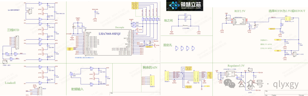
 01. The reference design of LHA7668 uses capacitive and inductive circuits to process and eliminate interference between analog ground and digital ground;02. The reference design of LHA7668 uses a 10nF capacitor coupled with AVSS for single-ended input, and a 100nF coupling for differential channel input; in practical use, such a design can achieve good hardware filtering effects;6. Explanation of Host Computer Access Code
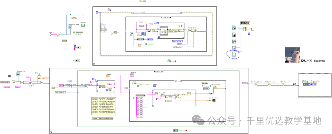 01. This code consists of two processes; the upper part is the code for parsing user operation [events], and the lower part is the [producer model] for serial data reception;02. [Upper Part] is a while loop with event structure + global shared dynamic events;02. Since the [main program] needs to control this event, the event operation address handle is placed in the global variable handle, and a dynamic event is created to allow the program to autonomously trigger and user operations; The main program operates the global handle to open the device and start/stop the device;03. [Lower Part] is while + serial interrupt trigger + command parsing + restoration and forwarding03. The serial event trigger combined with polling acquisition is the design method for the serial port; note that after the serial reception event is triggered, the trigger flag should be cleared first;04. [The code snippet in the upper right corner] functions to select the static VI address of the device to be connected by the main program, which can be understood as selecting who acts as the [producer] to produce data;7. Declaration01. The copyright of this tutorial’s hardware/manual/code belongs to Linghuixichip; thanks to Linghuixichip for their software and hardware support and assistance;02. The experimental data/software access/PCB-related technology of this tutorial belongs to Qianli Youxuan Teaching Base;02. This tutorial is for technical sharing,applied in the field of education; related code and technical discussions are for reference only;03.Note: High-definition images can be viewed via the mobile WeChat client;