【Content Directory】
1. Overview
2. Technical Sub-Forum Report Sharing
1. Advanced lithography technology for RF HEMT device manufacturing
2. Key technologies for large-size silicon-based III-nitride epitaxy
3. Research on new silicon-based IV group short-wave infrared detector devices and imaging arrays
4. Programmable photonic chips
3. Summary
【Recommended by Bay Semiconductor Exhibition】Related companies mentioned in this article
Jiufengshan Laboratory, Institute of Semiconductors, Chinese Academy of Sciences, Belgium Microelectronics Research Center.
1.Overview
On April 23, the third Jiufengshan Forum and Compound Semiconductor Industry Expo opened in Wuhan Optics Valley.This conference was hosted by the China Third Generation Semiconductor Industry Technology Innovation Strategic Alliance (CASA) and Jiufengshan Laboratory.
At the opening ceremony, Academician of the Chinese Academy of Engineering and President of Huazhong University of Science and Technology You Zheng, and Chairman of the China Semiconductor Industry Association Chen Nanxiang delivered speeches. Academician You Zheng stated that compound semiconductors, with their high photoelectric conversion efficiency and power performance advantages, have become a core support in strategic fields such as new energy vehicles and quantum technology. Chairman Chen Nanxiang indicated that China’s compound semiconductor industry is developing rapidly under the pull of market demand, forming a cluster of leading enterprises with international competitiveness.
In addition to exhibitions, this expo also set up11 parallel forums and10+ thematic seminars, allowing industry experts to fully communicate and enhance connections among peers..
2.Technical Sub-Forum Report Sharing
The sub-forum included11 sessions, covering key materials for compound semiconductors, core equipment for compound semiconductors,EDA tools and ecosystem, optoelectronic technology, power electronic technology, wireless electronic technology, advanced display technology, heterogeneous integration technology, neuromorphic and brain-like technology, advanced semiconductor testing technology, and the evaluation and standardization of third-generation semiconductor products.
1. Advanced lithography technology for RF HEMT device manufacturing
The head of lithography technology R&D at Jiufengshan Laboratory, Xiang Shili, shared the report titled “Advanced Lithography Technology for RF HEMT Device Manufacturing.” This report compared the advantages and disadvantages of ultraviolet lithography, nanoimprint, and electron beam exposure technologies in micro-nano processing, introduced the current status and demand of domestic lithography technology, and showcased the super-resolution advanced lithography technology (SRAL, see Figure 1).SRAL technology aims to break the limit resolution of existing DUV lithography machines to achieve smaller size micro-nano processing. Jiufengshan Laboratory successfully fabricated a gate length=85nm T-gate structure (commonly used in high mobility RF devices), see Figure 2.
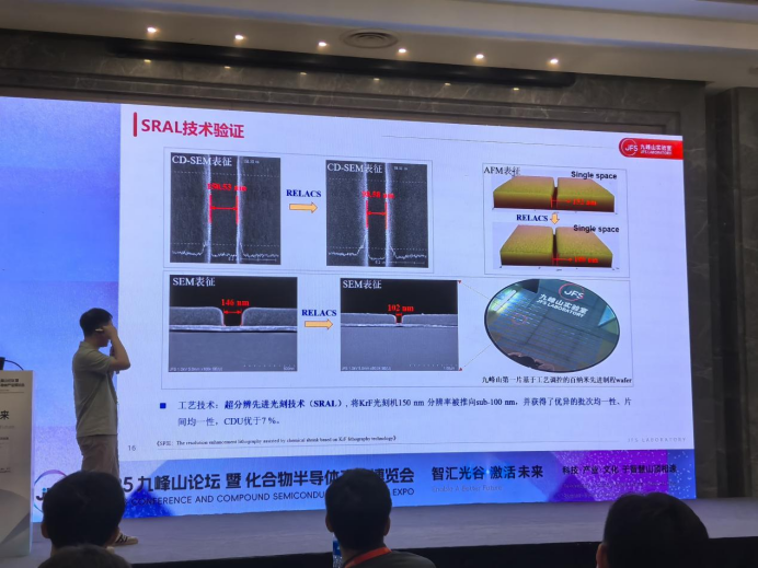
Figure1 Demonstration of Jiufengshan Laboratory’s super-resolution advanced lithography technology
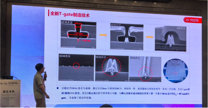
Figure2 T-gate structure manufactured by Jiufengshan Laboratory based onSRAL technology
2. Key technologies for large-size silicon-based III-nitride epitaxy
The epitaxy expert at Jiufengshan Laboratory, Lu Shuangzan, shared the report titled “Key Technologies for Large-Size Silicon-Based III-Nitride Epitaxy.” This report analyzed the market status and development trends ofGaN (Figure 3), and showcased theIII nitride MOCVD epitaxy (Figure4) andPA-MBE epitaxy (plasma-assisted molecular beam epitaxy technology, Figure5) technological achievements, which can successfully prepare high-quality, size-controllable GaN epitaxial thin film devices with good ohmic contact characteristics.
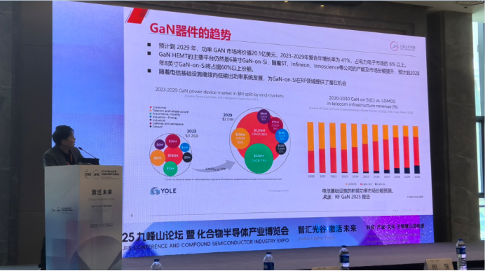
Figure3 Market status and development trends of GaN devices
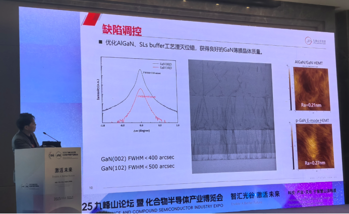
Figure4 MOCVD epitaxyGaN layer dislocation defect density characterization
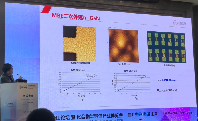
Figure5 PA-MBE secondary epitaxyn type heavily dopedGaN thin film morphology and the resistance test results of the ohmic contact interface
3. Research on new silicon-based IV group short-wave infrared detector devices and imaging arrays
Professor Xue Chunlai from the Institute of Semiconductors, Chinese Academy of Sciences, shared the report titled “Research on New Silicon-Based IV Group Short-Wave Infrared Detector Devices and Imaging Arrays.” This report analyzed the advantages of silicon-based IV group alloy material systems for short-wave infrared detector devices (Figure 6) and bottleneck issues (Figure 7), and showcased the pixel performance of the fabricated focal plane array. Based on the pixel performance of the detector using silicon-based IV group alloy material systems, it has approached the pixel performance of commercially available indium gallium arsenide detectors (Figure 8).
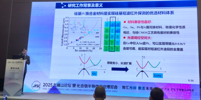
Figure6 Advantages of silicon-based IV group material systems
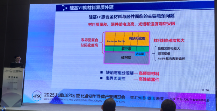
Figure7 Bottleneck of silicon-based IV group material systems
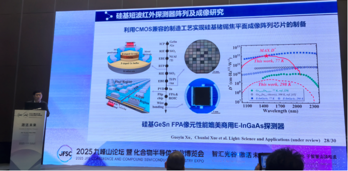
Figure8 Pixel performance of short-wave infrared detectors based on silicon-based IV group material systems
4. Programmable photonic chips
Programmable photonic chips (PIC) are one of the hot topics in semiconductor research in recent years. Traditional chips use electronic processing and transmission of signals, while photonic chips utilize photons for transmission and processing of signals, offering advantages such as low energy consumption, low transmission delay, high processing speed (up to10~100 times faster than electronic chips), and strong resistance to electromagnetic interference. However, due to manufacturing difficulties, development cycles, and cost issues, they are still mainly in the research stage.
Professor Wim Bogaerts from the Belgium Microelectronics Research Center (IMEC) shared the report titled “Programmable Photonic Chips.” He presented a schematic diagram of the structure of photonic chips (Figure 9), as well as the physical results of photonic chips produced by Professor Wim Bogaerts’ research group (Figure 10).
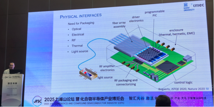
Figure9 PIC schematic diagram
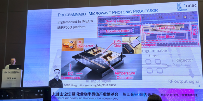
Figure10 PIC physical image, modular labeling completed
3.Summary
This exhibition covers an area of20,000 square meters, with nearly300 companies showcasing their products, including well-known domestic and international companies, research institutes, and universities such as Northern Huachuang, Huada Jiutian, Innosilicon,IMEC, etc., comprehensively displaying innovative achievements in core links of the industrial chain from materials, equipment,EDA to manufacturing, covering the entire industrial chain of “materials-equipment-manufacturing-application,” and further strengthening the industrial agglomeration effect of Optics Valley.

Chip to Empower the Future, Smart Innovation Ecosystem
Bay Semiconductor Exhibition 2025 looks forward to seeing you!