Printed Circuit Board
Advanced PCB Design
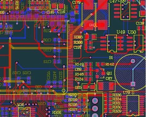
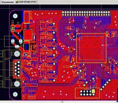
Advanced design of Printed Circuit Boards (PCBs) requires a combination of engineering practice, signal integrity analysis, electromagnetic compatibility (EMC) design, and manufacturing processes. The following are the core points and practical tips for advanced design to help you enhance the professionalism and reliability of PCB design.
1.High-Speed Signal and Signal Integrity (SI) Design
Differential Pairs and Impedance Control
High-speed signals (such as USB, HDMI, PCIe) should use differential pair design, maintaining symmetrical routing and avoiding length differences (recommended <5mil).
Calculate and control characteristic impedance (such as 50Ω single-ended, 100Ω differential), using impedance calculation tools (such as PolarSi9000).
Crosstalk and Reflection Suppression
Increase signal spacing (3 times the line width or more), avoiding long parallel traces.
Terminal matching (series resistors, termination resistors) reduces signal reflection.
Reference Plane Continuity
Below high-speed signal paths, a complete ground plane must be maintained to avoid crossing splits (SplitPlanes).
2. EMC/EMI Optimization Design
Ground Plane and Power Segmentation
In multilayer boards, use a “complete ground plane” as a reference layer to avoid ground loops.
Digital and analog areas should be isolated by ferrite beads or 0Ω resistors, with single-point connection to the ground plane.
Filtering and Shielding
Add π-type filters or ferrite beads to critical signal lines (such as clock lines).
Use shielding covers or grounded copper foil in sensitive circuit areas.
Edge Radiation Control
Avoid placing high-speed signal lines near the board edge, and if necessary, add ground trace wrapping (GuardTrace).
3.Multilayer Board Design Techniques
Stacking Structure Optimization
A typical 4 layer board:TopSignal→GND→Power→BottomSignal.
6 layer board recommendation:Signal1→GND→Signal2→Power→GND→Signal3.
Power Integrity (PI) Design
Power planes should use a “grid” or “solid copper” structure to reduce impedance.
Decoupling capacitors should be placed close to power pins (such as 0.1μF ceramic capacitors +10μF tantalum capacitor combination).
4.Thermal Management Strategies
Thermal Via Arrays
Add thermal vias under high-power devices (such as LDO, MOSFET) to connect to internal ground planes for heat dissipation.
Via diameter should be ≥0.3mm, filled with thermally conductive epoxy (for high-power scenarios).
Heat Sink Pads and Copper Foil
Use large copper foil areas to expand heat dissipation area, and add heat sinks or fans if necessary.
Thermal Simulation Analysis
Use tools (such as ANSYSIcepak) to verify thermal distribution and avoid local overheating.
5.Design for Manufacturability (DFM) and Assembly (DFA)
Pad and Solder Mask Design
Avoid overly small pads (such as 0402 package pads ≥0.5mm).
Solder mask openings should be larger than pads by 0.1mm, to prevent solder bridging.
Component Layout Rules
Leave repair space (≥5mm) around high-density BGA devices.
Polarized components (such as electrolytic capacitors) should have a uniform orientation for automated assembly.
Panelization and Process Edges
Irregular board shapes should add process edges (≥5mm), Vcut or tab routing.
6.Simulation and Verification Tools
Signal Integrity Simulation
Tools:HyperLynx, CadenceSigrity, ADS.
Analyze eye diagrams, rise times, and timing margins.
Power Integrity Simulation
Verify PDN (Power Distribution Network) impedance, with target impedance ≤ target frequency range requirements.
3D Electromagnetic Field Simulation
Use CST, HFSS to analyze EMI radiation of complex structures.
7.Advanced Packaging and Special Processes
BGA/Micro-pitch Device Design
Use blind/buried vias (Blind/BuriedVia) or HDI processes (line width/line spacing ≤3mil).
Fan-out design: Prefer “dog-bone” or “escape routing”.
Rigid-Flex PCB
Avoid right-angle routing in bending areas, using arc transitions instead.
Dynamic bending areas should use polyimide substrates.

8.Design Specifications and Standardization
IPC Standards Reference
IPC2221B (General Design Standards), IPC7351B (Pad Design Standards).
IPCA600 (Acceptance Standards), IPC6012 (Rigid Board Performance Specifications).
Design Rule Check (DRC)
Set multilayer rules: line width, spacing, via types, silkscreen clarity, etc.
9.Automation and Scripting Applications
EDA Tool Script Development
Use Python or Skill languages to write scripts (such as AltiumDesigner scripts), for batch modification of packages and report generation.
Automatically generate impedance calculation tables, BOM comparison tools.
10.Case Study Analysis
Case1: High-Speed DDR4 Routing
Equal length group control (data lines ±50mil, address/control lines ±100mil).
Ensure reference plane continuity, avoiding crossing power splits.
Case2: RF Circuit Design
50Ω microstrip design, using coplanar waveguides (CPWG) to reduce losses.
Ensure clear space in the antenna area, prohibiting copper pouring.
Advanced PCB design requires a combination of theory and practice, through simulation verification, DFM optimization, and problem retrospectives, gradually enhancing design capabilities. It is recommended to start with complex projects, accumulate experience, and continuously optimize the design process.
END