TOP.10Click to view recent hot articles
Summary of the evolution of semiconductor technology from 180nm to 14nm
What is semiconductor WAT testing?
Analysis of the current supply and demand situation of semiconductor manufacturing talent in China
The advanced process journey of TSMC: from N7 to N2
Evolution and core principles of Intel’s advanced process technology
Advanced packaging mainstream technologies through the lens of the three giants
In-depth report on 2.5D and 3D packaging technologies
Comprehensive analysis of semiconductor core component electrostatic chucks
Technical analysis of semiconductor particle detection equipment
Technical principles of semiconductor film thickness detection equipment
This public account is dedicated to sharing analyses related to semiconductors and industry communication. The latest public account push policy will not push articles from accounts you follow; you need to set a star mark to receive pushes. Therefore, if you do not want to miss the wonderful content of this public account, please be sure to mark it as a star. Thank you.More high-quality semiconductor content, information reports, and workplace skills are published on Knowledge Planet. If interested, please scan the code to join. Semiconductor Industry Knowledge Circle
Downloadable files: 3000+ copies
Continuous sharing of files: 20T+
Semiconductor technology, industry reports
Workplace culture and capabilities
Content
Semiconductor components refer to parts that meet the technical requirements of semiconductor equipment in terms of materials, structure, process, quality, precision, reliability, and stability. They are the foundation and core of semiconductor equipment, directly determining the reliability and stability of the equipment.
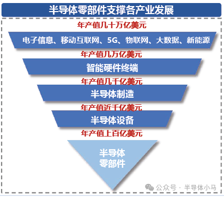
Semiconductor components are key to supporting the exponential growth of downstream industries. Precision semiconductor components are not only one of the more challenging and technically demanding aspects of semiconductor equipment manufacturing but also one of the bottlenecks for domestic semiconductor equipment companies. As a key to the evolution of core semiconductor technology, semiconductor components support the chip manufacturing industry and smart hardware terminals, thereby supporting the entire modern electronic information industry. In terms of output value, the annual output value of components reaches hundreds of billions of dollars, driving an exponential growth trend in the scale of downstream industries.
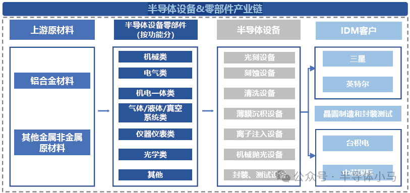
The supply chain connects materials and equipment, and supply shortages hinder equipment delivery. Semiconductor components are positioned between raw materials and semiconductor equipment in the industrial chain, with direct customers being equipment manufacturers, wafer fabs, or IDM customers. During an economic upturn, shortages of components often restrict equipment manufacturers’ ability to deliver on time. According to TrendForce data, in the first half of 2022, semiconductor equipment delivery times faced extensions of 18-30 months, with component shortages being a significant pain point.
 PART01
Characteristics of Semiconductor Components
The semiconductor component industry typically features high technology intensity, interdisciplinary integration, a small and fragmented market share, yet plays a crucial role in the value chain.
1) Technology-intensive, with high precision and reliability requirements:
Due to the application of semiconductor components in precision semiconductor manufacturing, their cutting-edge technology-intensive characteristics are particularly evident compared to basic components in other industries, featuring high precision, small batch sizes, diverse varieties, special dimensions, complex processes, and extremely stringent requirements.
Semiconductor component companies often need to balance composite functional requirements such as strength, strain, corrosion resistance, electronic properties, electromagnetic properties, and material purity during the production process, resulting in extremely high technical barriers.
2) Interdisciplinary integration, with high demand for composite technical talent:
There are many types of semiconductor components, covering a wide range, and the industrial chain is long. Their R&D design, manufacturing, and application involve interdisciplinary and multidisciplinary integration, thus there is a significant demand for composite talent.
3) Significant market fragmentation characteristics:
Compared to the semiconductor equipment market, the semiconductor component market exhibits significant fragmentation characteristics, with a small market space for single products and high technical barriers. Therefore, leading international semiconductor component companies typically adopt a cross-industry, multi-product line development strategy, and continuous mergers and acquisitions are the main means of expansion for leading international semiconductor component companies.
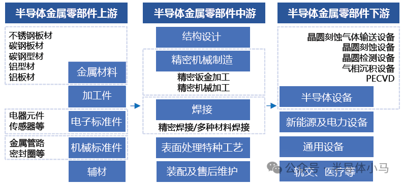
Semiconductor equipment features a variety of products, small batches, and customization, while semiconductor components also share similar characteristics, with numerous subcategories, small batches, high precision, and complex processes. According to data from Chip Research, the main components with a significant proportion of procurement costs for mainland wafer fabs include quartz components, RF generators, various pumps, etc., accounting for over 10%. Additionally, various valves, chucks, shower heads, edge rings, and other components also have a high procurement proportion.
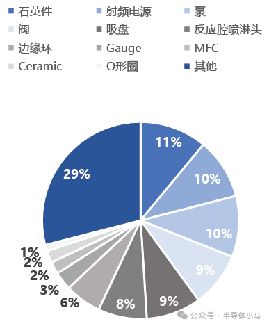
Structure of equipment component procurement by Chinese wafer fabs (8-12 inches)
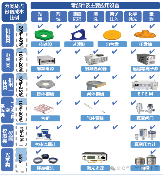
Classification of semiconductor equipment components and main application devices
PART02
Classification of Semiconductor Components
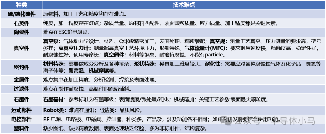
According to the main materials and functions of semiconductor components, they can be divided into twelve categories, including silicon/silicon carbide components, quartz components, ceramic components, metal components, graphite components, plastic components, vacuum components, sealing components, filtering components, moving components, electronic control components, and other components.
 PART03
Semiconductor Plastic Components
Plastic products run through the entire semiconductor manufacturing production line and are widely used in wafer manufacturing, transfer, transportation, storage, cleaning, and other steps.
1)Used for cleaning on the production line
Main types: carriers, racks, etc.
Materials: This type of packaging container is mostly made of fluorine-containing materials (such as PFA, PTFE, PVDF) and PEEK materials.
Usage conditions: strong acids, strong bases, high temperatures
2)Used for transfer on the production line
Main types: carriers, transfer racks, etc.
Materials: Mostly made of PP, PEEK, and other materials.
Requirements: Good dimensional stability, some with anti-static requirements, usage conditions at room temperature.
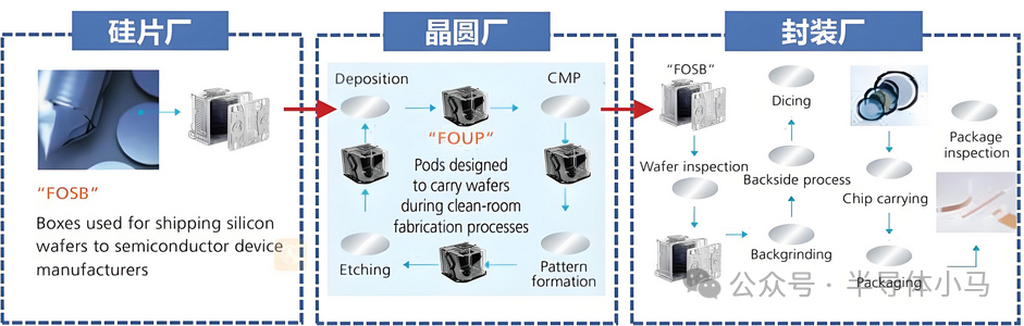
3)Used for transportation and storage packaging
Main types: Wafer Box/FOUP/FOSB
Materials: Made of PP, PBT, PEEK, and other materials.
Requirements: Certain mechanical strength, high chemical purity, to avoid secondary contamination of the packaged items during use.
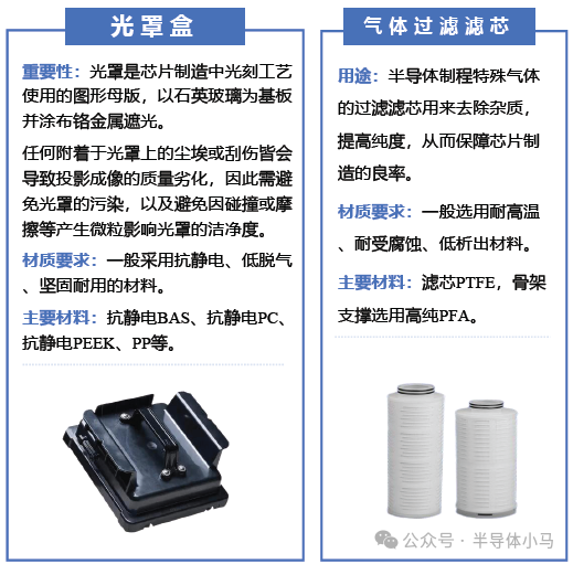
Semiconductor plastic consumables play different roles in different process stages, need to meet different material requirements, and adopt different plastic materials, making them indispensable throughout the entire process. Taking typical plastic products such as wafer carriers, CMP retaining rings, photomask boxes, and gas filter elements as examples:
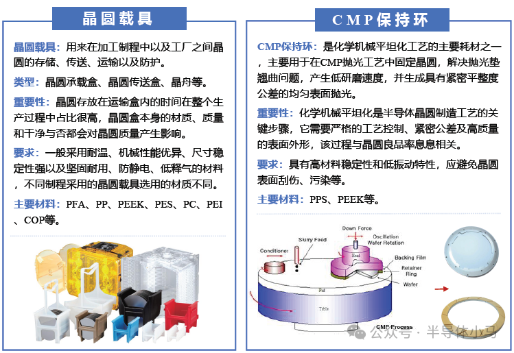
Plastic components — Wafer carriers
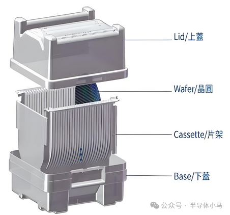
Wafer carriers are important semiconductor plastic products used for silicon wafer production, wafer manufacturing, and storage, transportation, and protection of wafers between factories. They are essential components for constructing automated handling solutions for 12-inch wafer fabs in the AMHS (Automated Material Handling System).
During the manufacturing process, chips generally need to travel back and forth on the semiconductor production line hundreds of times within three weeks, and the time wafers spend in transport boxes is significant throughout the production process. Therefore, wafer carriers are indispensable tools for protection and transportation throughout the entire production process.
Chips are expensive and easily affected by misoperation and contamination, and the material, quality, and cleanliness of the wafer carriers themselves can significantly impact wafer quality, playing an important role in the chip manufacturing process.
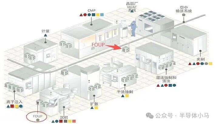
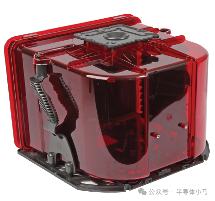
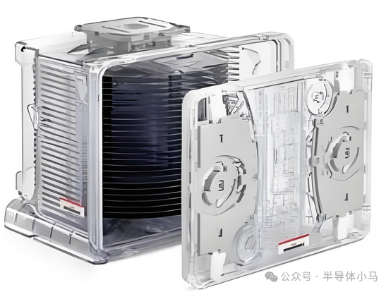
There are many types of wafer carriers, each with its applications, with the main wafer carriers being FOUP and FOSB:
FOUP (Front Opening Unified Pod): Mainly used for the protection, transportation, and storage of wafers in fabs, it is an important transport container for the automated transfer system specific to 12-inch wafer fabs.
Function: Generally holds 25 wafers, protects wafers, isolates external dust contamination, thereby improving yield.
Structure: Each FOUP has various connection plates, pins, and holes to ensure it is positioned at the loading port and manipulated by the AMHS system.
Materials: It is made of low outgassing materials and low moisture absorption materials, significantly reducing the release of organic compounds to prevent contamination of wafers; at the same time, excellent sealing and inflation functions provide a low-humidity environment for the wafers. Additionally, FOUPs can be designed in different colors, such as red, orange, black, transparent, etc., to meet process needs and distinguish different processes and procedures: generally, FOUPs are customized by customers based on differences in fab production lines and equipment.
FOSB (Front Opening Shipping Box): Mainly used for the transportation of 12-inch wafers between silicon wafer manufacturing plants and fabs.
Function: FOSB generally holds 25 wafers, and can be operated automatically by the AMHS system or manually.
Characteristics: Due to the large size of wafers and higher cleanliness requirements, special positioning pieces and shockproof designs are used to reduce impurities generated by wafer displacement and friction.
Materials: The raw materials are made of low outgassing materials, which can reduce the risk of gas release contaminating the wafers. Compared to other wafer transport boxes, FOSB has better airtightness. Additionally, in back-end packaging line fabs, FOSB can also be used for the storage and transfer of wafers between various processes.
 PART04
Semiconductor Metal Components
Companies producing semiconductor metal components belong to the precision metal manufacturing industry. The raw materials mainly include aluminum, stainless steel, carbon steel, copper, and other metals, with products primarily being customized precision metal structural parts characterized by “small batch, diverse varieties, complex processes, and high precision,” mainly applied in high-end semiconductor etching, deposition, wafer inspection, and other equipment.
Profitability is significantly affected by fluctuations in upstream metal material prices, and it is expected to gradually gain control over raw material prices in the future.
The industry exhibits significant economies of scale, where expanding scale can significantly reduce the unit cost of products.
The semiconductor vertical division of labor model has specialized the industrial chain, forming vendors specialized in IC design, wafer foundry, packaging testing, and specialized semiconductor equipment and material suppliers.
Classification of semiconductor metal components
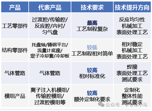
Semiconductor metal components can be divided into four categories:
1) Process components: Directly contact or participate in reactions with wafers.
2) Structural components: Serve functions such as connection, support, and cooling, without reacting.
3) Gas pipelines: Transport pipelines connecting gas sources to reaction chambers.
4) Module products: Achieve part of the core functions of semiconductor equipment after assembly.
Structure of the semiconductor metal components industry
Technical requirements for semiconductor metal components
PART05
Semiconductor Ceramic Components
Ceramic components are semiconductor equipment components made from advanced ceramic materials such as alumina ceramics, aluminum nitride ceramics, and silicon carbide ceramics through precision processing.
Advanced ceramic materials exhibit excellent performance in strength, precision, electrical properties, and corrosion resistance, meeting the complex performance requirements of semiconductor manufacturing in vacuum and high-temperature environments.
Precision ceramic components are widely used in core equipment for several key semiconductor manufacturing processes, such as lithography, etching, thin film deposition, ion implantation, CMP, etc., playing roles in support, protection, and flow guidance, especially within the equipment chamber.
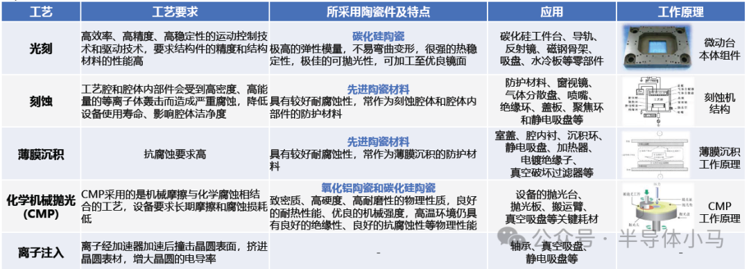
Ceramic components in key semiconductor manufacturing processes
Semiconductor ceramic components —Electrostatic chucks
Electrostatic chucks are ultra-clean wafer carriers suitable for vacuum or plasma environments. They utilize the principle of electrostatic adsorption to uniformly hold ultra-thin wafers, and also play a role in heat dissipation, using the thermal conduction system of the electrostatic chuck and the helium gas flow to dissipate heat generated during processing. This product is widely used in high-end semiconductor manufacturing equipment such as PVD, PECVD, ETCH, EUVL, and ion implantation. The lifespan of electrostatic chucks generally does not exceed two years, making them consumables with a high replacement rate.
The basic principle of electrostatic chucks is to achieve wafer adsorption through the attractive force of opposite charges, with the main structure being a sandwich structure consisting of a dielectric layer, an electrode layer, and a substrate layer.
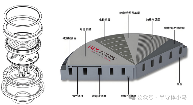
According to the materials of the dielectric layer, electrostatic chucks are mainly divided into Coulomb-type and Johnsen-Rahbek-type (JR-type). Due to the closer proximity of opposite charges, Johnsen-Rahbek-type electrostatic chucks can achieve the same adsorption force at lower voltages.
| Parameter | Coulomb-type | Johnsen-Rahbek type (JR type) |
|---|---|---|
| Dielectric Material | Pure ceramics (e.g., Al₂O₃), pure dielectrics (high impedance) | Doped dielectrics (e.g., doped AlN ceramics), semiconductor materials |
| Driving Voltage | 3000–5000V (high voltage) | 500–800V (low voltage) |
| Adsorption Force | Moderate (depends on polarized charge) | Strong (depends on interface charge accumulation) |
| Response Time | >100ms | <50ms |
| Temperature Control Capability | Single-zone/few-zone temperature control | Supports multi-zone independent temperature control (accuracy ±0.5℃) |
| Advantages | Excellent dielectric insulation, high charge stability | Low voltage drive energy consumption, adsorption force is 3-5 times that of Coulomb type |
| Disadvantages | High voltage power supply can easily cause Joule heating, slow response speed | Doping of dielectrics can easily introduce impurities, residual charge during desorption is difficult to eliminate |
| Typical Applications | Low-stress thin film deposition (e.g., initial layers of PECVD) | Plasma etching, PVD metallization (high-temperature process scenarios) |
For details on electrostatic chucks, please refer to previous articles:
Comprehensive analysis of the electrostatic chuck technology of semiconductor core components, this thing costs over 1 million or even 2 million!
Analysis of the adsorption and desorption mechanisms of electrostatic chucks in semiconductor equipment: how does it prevent wafers from “sticking”?
The electrostatic chuck industry is highly concentrated, with American and Japanese manufacturers dominating. The top three global electrostatic chuck market revenue leaders are Applied Materials (USA), Lam Research (USA), and Shinko Electric (Japan), accounting for approximately 40%, 30%, and 10% of the market, respectively. The electrostatic chucks produced by Applied Materials and Lam Research mainly supply their own semiconductor equipment, while Shinko Electric, TOTO, and NTK supply third-party vendors. Currently, domestic companies Beijing Huazhuo Jingke and Guangdong Haituo Innovation have achieved mass production and commercialization of electrostatic chuck products.
We will introduce other categories later, and the full text has been uploaded to Knowledge Planet. Interested friends are welcome to read and download on Knowledge Planet:

Note: Some information is sourced from the internet; please delete if infringing.

 Semiconductor Pony
WeChat ID: SEMI147
Communication, consultation, group joining

💕In-depth light reading
—- Strongly recommended for engineers’ advancement —-
Oxidation diffusion process (download link at the end)Chemical vapor deposition (download link at the end)Physical vapor deposition (download link at the end)Coating exposure development (download link at the end)Dry etching process (download link at the end)Injection equipment process (download link at the end)Chemical mechanical polishing (download link at the end)Wet etching process (download link at the end)