1.Problem Description
An industrial display screen experienced a blue screen phenomenon and system freeze during ESD (Electrostatic Discharge) testing, where ±6kV contact discharge was applied to the network port, USB, and serial port. The system could be restored by rebooting, but the test failed.
This issue has persisted for six months, during which the client company and the solution provider have made four revisions (from V1.0 to V1.31), investing significant manpower and resources without resolution. Time is of the essence.
2.Fault Diagnosis
Considering that previous modifications to the board addressed grounding, filtering, and isolation without improvement, it was suspected that the board had ESD vulnerabilities. Therefore, a sensitive source diagnosis and remediation plan was determined to thoroughly resolve the issue from the source.
Based on the experimental phenomena, it was determined that the CPU functional unit was being interfered with. Analyzing the signal pins of the core sub-board (CPU module circuit) from practical experience and signal functionality, it was concluded that the signals listed in Table 1 are particularly sensitive and prone to ESD interference.
Table 1: Sensitive Signals Prone to ESD Interference
|
Index |
Network Name |
Signal Function |
ESD Sensitive |
|
1 |
LCD_HSYNC |
LCD horizontal sync signal |
YES |
|
2 |
LCD_VSYNC |
LCD vertical sync signal |
YES |
|
3 |
I2C_SDA |
I2C bus bidirectional data signal |
YES |
|
4 |
I2C_CLK |
I2C bus clock signal |
YES |
|
5 |
LCD_EN |
LCD enable signal |
YES |
|
6 |
LCD_CLK |
LCD clock signal |
YES |
|
7 |
VCC_3V3_MPU |
3.3V power supply for MPU unit |
YES |
|
8 |
eDP_RESET |
eDP interface reset signal |
YES |
The ESD gun voltage was adjusted to 100V, 300V, 600V, and 1000V, and contact discharge was applied to the signal pins listed in Table 1 on the core sub-board to identify ESD sensitive signals, as shown in Figure 1.
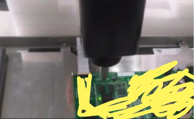
Figure 2: Contact Discharge on IC Pins
During the experiment, the issue did not recur, thus ruling out problems with these signals. The test records are shown in Table 2.
Table 2: ESD Sensitive Signal Verification Results
|
Index |
Network Name |
100V |
300V |
600V |
1000V |
|
1 |
LCD_HSYNC |
Normal |
Normal |
Normal |
Normal |
|
2 |
LCD_VSYNC |
Normal |
Normal |
Normal |
Normal |
|
3 |
I2C_SDA |
Normal |
Normal |
Normal |
Normal |
|
4 |
I2C_CLK |
Normal |
Normal |
Normal |
Normal |
|
5 |
LCD_EN |
Normal |
Normal |
Normal |
Normal |
|
6 |
LCD_CLK |
Normal |
Normal |
Normal |
Normal |
|
7 |
VCC_3V3_MPU |
Normal |
Normal |
Normal |
Normal |
|
8 |
eDP_RESET |
Normal |
Normal |
Normal |
Normal |
Continuing to analyze the sensitive circuits on the core sub-board, the issue recurred when contact discharging the sensitive signal DDR_CLK at 100V, and the problem could be reproduced with each discharge.
The DDR_CLK wiring is 4 mil, and no pads were reserved for the wiring, limiting remediation options. To determine whether the electrostatic radiation electromagnetic field affects the DDR_CLK clock signal, a metal grounding wire was placed directly above the DDR_CLK line, and the ESD gun was used to discharge onto the copper terminal of the grounding wire, as shown in Figure 3.
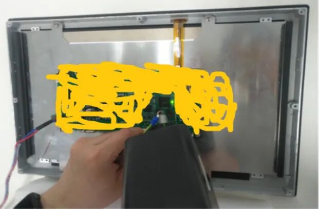
Figure 3: Contact Discharge on Grounding Wire Copper Terminal
Using the method shown in Figure 3, during 6kV contact discharge, the problem could be reproduced in all five discharges. Therefore, it was confirmed that the electrostatic electromagnetic field radiation affects the DDR_CLK signal and DDR devices. At this point, copper foil was used to shield the core board area and ground it, protecting the sensitive DDR signals and modules, as shown in Figure 4.
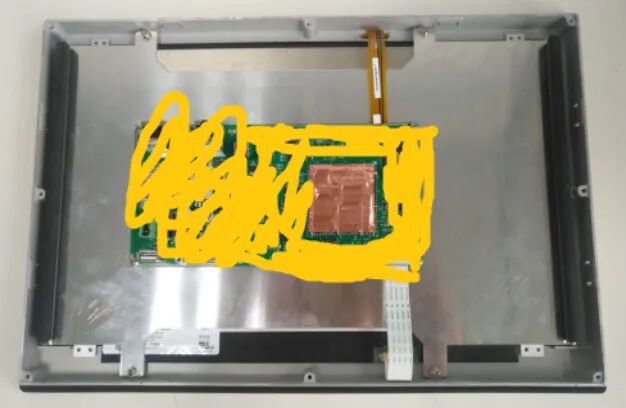
Figure 4: Core Board Module Shielding
After shielding the core board module area, contact discharges of ±6kV, 8kV, and 10kV were applied to the I/O interfaces, with each series of 40 discharges resulting in normal system operation, thus resolving the issue. It was determined that the core board was affected by electrostatic interference, causing the entire system to freeze.
3.Cause Analysis
Continuing to verify whether the entire system ESD was due to radiation coupling or capacitive coupling, analysis showed that the system’s electrostatic discharge leakage path was I/O interface — single board PGND — metal liner — metal chassis — chassis cover — grounding wire, as shown in Figure 5.
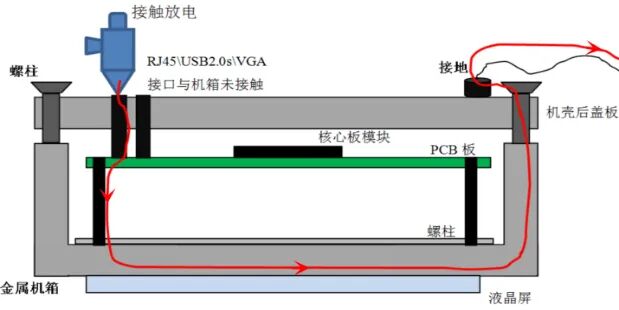
Figure 5: System Electrostatic Discharge Leakage Path
When the chassis cover was not screwed to the metal chassis or was left uncovered, it was found that there were no issues with electrostatic discharge, thus ruling out radiation coupling. At this point, the electrostatic leakage path was I/O interface — single board PGND — metal liner — metal chassis, indicating that the sensitive parts of the core board DDR had no capacitive coupling with the chassis cover (the two are very close), as shown in Figure 6.
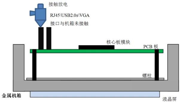
Figure 6: Electrostatic Leakage Path Without the Cover
Based on the above, a simplified model of the electrostatic coupling of the core sub-board is shown in Figure 7.
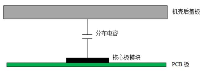
Figure 7: Core Sub-Board Electrostatic Coupling Model
During diagnosis, after adding a shielding cover to the core sub-board, the electrostatic coupling model is shown in Figure 8.
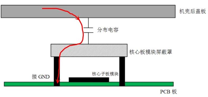
Figure 8: Core Sub-Board Electrostatic Coupling Model
From Figure 8, it can be seen that after adding a shielding cover to the core sub-board, the electrostatic energy from the chassis cover directly couples to the metal shield and is grounded through the shield’s grounding pin to GND, thus preventing ESD from directly coupling to the sensitive DDR module, resolving the issue. Therefore, based on the above analysis, the electrostatic interference from the chassis cover was determined to be capacitively coupled to the DDR module circuit, causing the ESD problem.
4.Remediation Measures
Since the core sub-board is a platform product of the client company, and the DDR circuit on the module is particularly sensitive, it is recommended that the mainboard adopt a shielding cover to shield the sensitive core sub-board module for mass production. This solution is simple and practical, with a cost increase of less than 0.5 yuan, and reliable results. After communicating with the client, it was confirmed that there is sufficient space on the mainboard for this solution, and the shielding cover is shown in Figure 9.
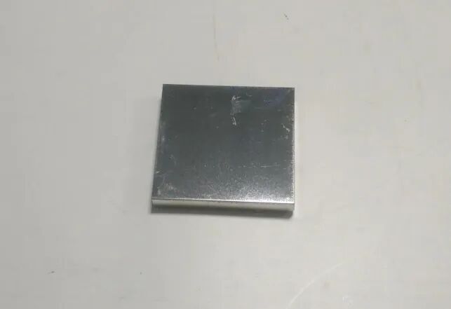
Figure 9: Core Board Shielding Cover
5.Practical Effects
After the board modification, ESD tests were conducted again, and the system freeze issue has not recurred, and the tests passed.
Summary
During ESD experiments, engineers often encounter issues where a single discharge causes a system freeze, and despite numerous PCB modifications, the problem remains unresolved, leading to frustration. Why? Because there are extremely sensitive weak points in the circuit regarding ESD. Without addressing the critical points, success is unattainable! In this case study, the ESD issue was identified through meticulous diagnosis and analysis, determining the sensitive sources and coupling paths, and successfully resolved by shielding the sensitive sources. This remediation method and thought process remind us that to defeat the enemy, one must strike at the heart; if one takes action, it must be decisive. The first battle is the decisive battle, determining the outcome.
