
Today, I would like to share with you:Buck Converter PCB Design
1. Buck Converter PCB Design Requirements
1. Buck Converter Design Requirements
The requirements for the buck converter are:
-
Input voltage from 4.5V to 17V
-
Adjustable output voltage from 0.76V to 7V
-
Maximum output current of 1A
2. Power Supply Requirements
-
Input voltage 7.0~14.0V
-
Output voltage 5.0V
-
Output current 1.0A
This is a typical requirement for a 5V power supply wall adapter, and you can use a 9V battery for power.
2. Schematic Design
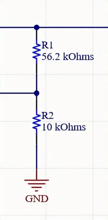
1. Output Resistor Selection
The TPS561208 is the main chip and the first step in the design is to select the output voltage resistors to set the output voltage to 5V.
The resistors can be calculated using the following formula:
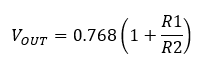
Resistor Calculation
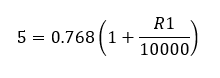
When selecting resistors, it is important to note that if the resistance value is relatively low, it means the converter is less susceptible to noise, but efficiency will decrease at low loads, so select R2 resistor value as 10k Ohm from the recommended table in the datasheet, and then calculate R1 value using the following formula:
R1 Value
R1 Value
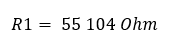
Since 55.104kΩ is not a standard resistor value, I chose 56.2 kΩ, which can provide an output of 5.08 V.
R1
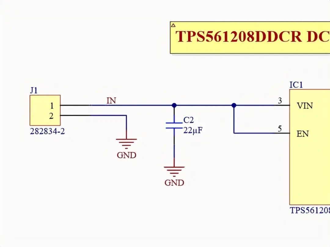
2. Input Capacitor Selection
The datasheet recommends an input capacitor of 10 uF or larger, so I chose a 22 uF capacitor because many 9V wall adapters have high noise.
Input Capacitor
3. Inductor Selection
Inductor selection is a bit tricky and is also chosen from the recommendations in the datasheet.
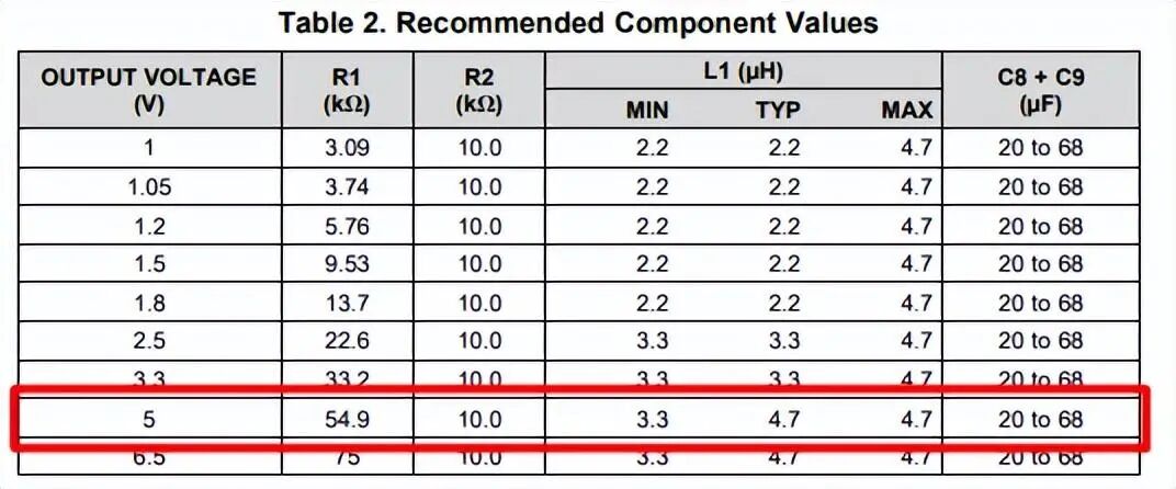
Recommended Component Values
It is important to choose an inductor with a saturation current and rated current not exceeding 1A.
4. Output Capacitor
To achieve a stable converter, it is recommended thatthe output capacitor be 20 to 68 uF. In this design, a single 47 uF capacitor was chosen.
It is essential to fully understand the power supply’s functionality to adjust values in a timely manner. For example, if the power supply load changes rapidly, a capacitor with a higher value needs to be added.
5. Bootstrap Capacitor
In addition to the input and output capacitors, a bootstrap capacitor is also required, and here I used a 0.1 uF ceramic capacitor.
6. Connectors
There are many options for connector selection, as there are no specified connection requirements. I chose the TE Connectivity 2-pin connector for easy wire connection and testing of the circuit board. The terminals are readily available for procurement and can be replaced with other connectors that have a 2.54mm pitch.
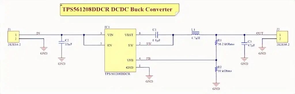
PCB layout designed for the TPS561208DDCR buck converter
3. Initial PCB Design
The initial PCB design had poor performance.

Initial PCB Design
The main issues were as follows:
1. No reference to the recommended layout and design tips in the datasheet.
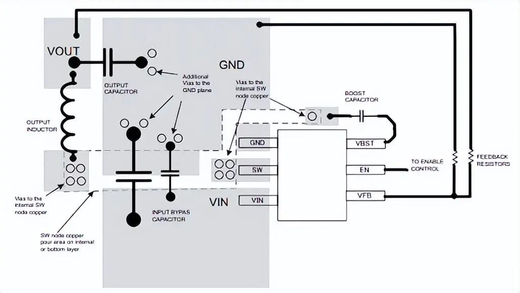
PCB layout example from the datasheet
2. The inductor and the switching path of the inductor loop were not properly routed, which could lead to excessive crosstalk and EMI issues.
The current loop layout of the switching regulator greatly affects the performance beyond just the stability of the regulator, potentially leading to high noise.
This shows the two current loops in the initial PCB design, input (blue) and output (red):
PCB layout of the input and output current loops for the first DC-DC buck converter design
The current path through the regulator should be as short and wide as possible to minimize radiated emissions.
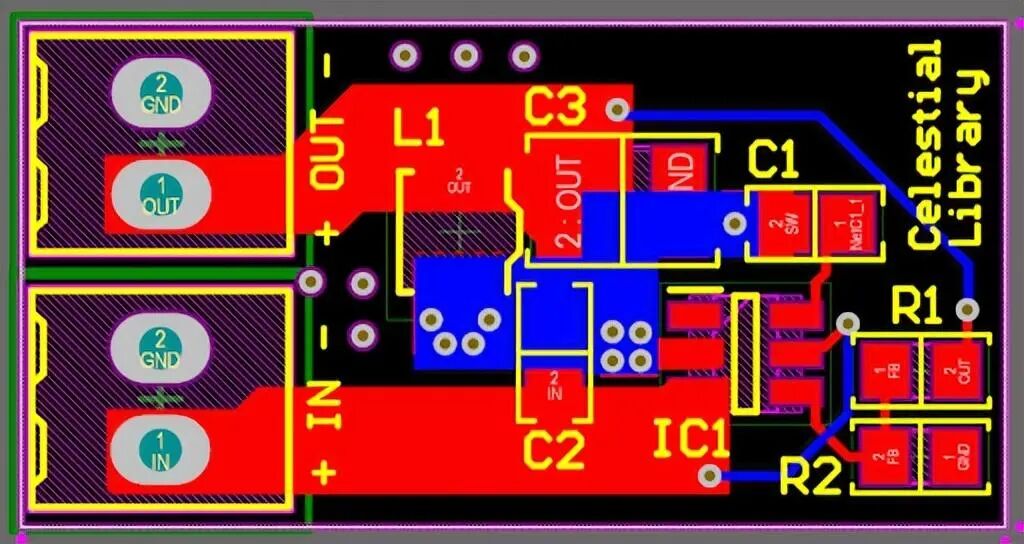
4. PCB Design Layout Improvements
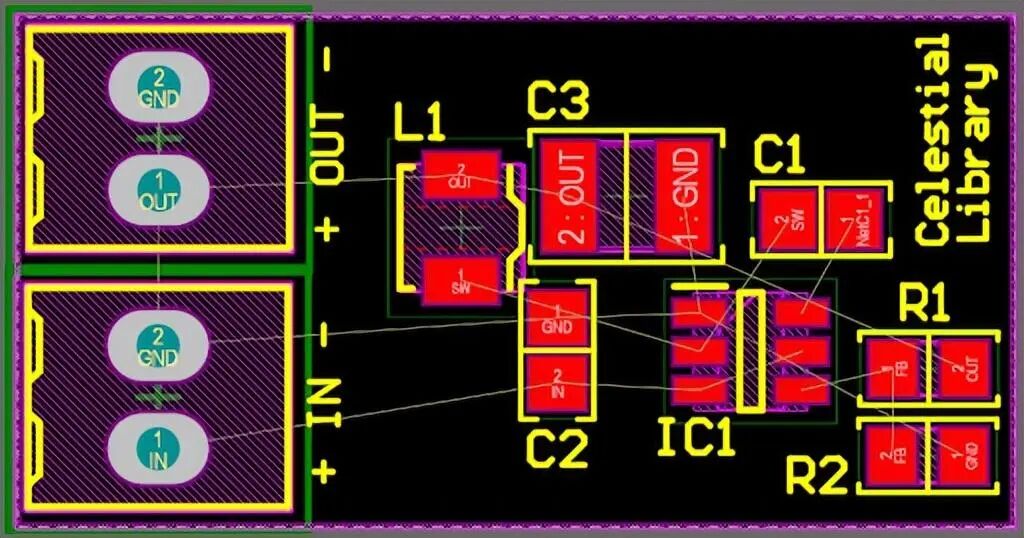
1. Component Placement
The first step in improving the PCB layout is to correctly position the components, and the component layout should also reference the layout in the datasheet, with slight modifications.
Referencing the recommended layout and design tips from the datasheet for component placement
2. Manual Routing
It is important to manually route the PCB instead of using automatic routing, as this allows you totrack the current flowing through the input and output loops and the circuit, so you can see how long the loops are and which direction the current flows.
PCB Manual Routing
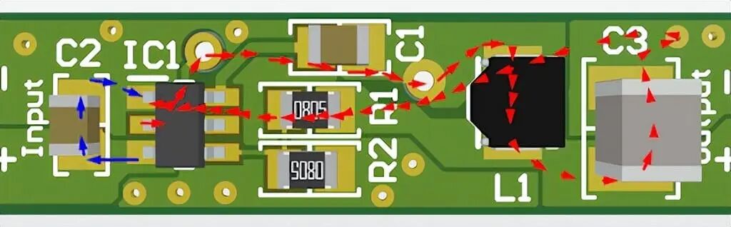
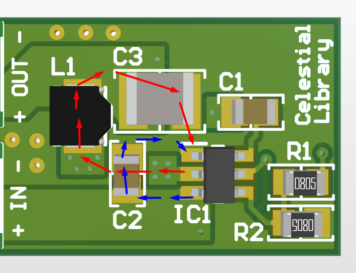
After manual routing, the current loops were reviewed, and while the input loop did not change much, the output loop showed significant improvement.
The input loop did not change much, but the output loop showed significant improvement
3. Adding a Ground Plane to Input and Output Loops for Low Impedance
Adding a Ground Plane
4. Adding Top and Bottom Layers
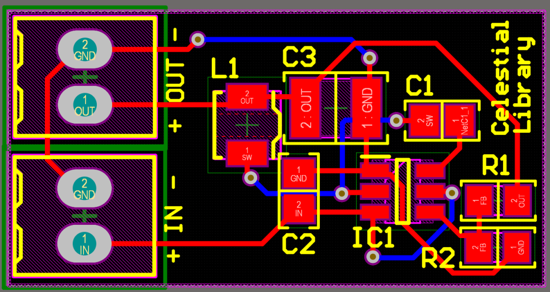
Finally, adding top and bottom layers, below is the improved PCB design layout for the buck regulator.
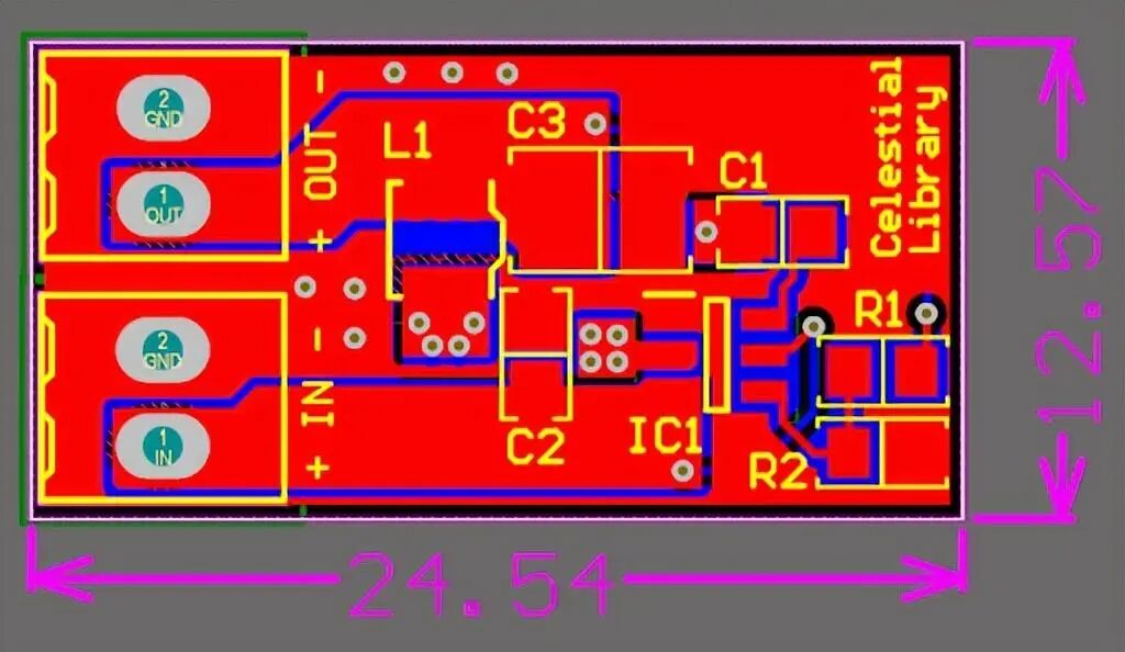
Improved PCB design layout for the buck regulator
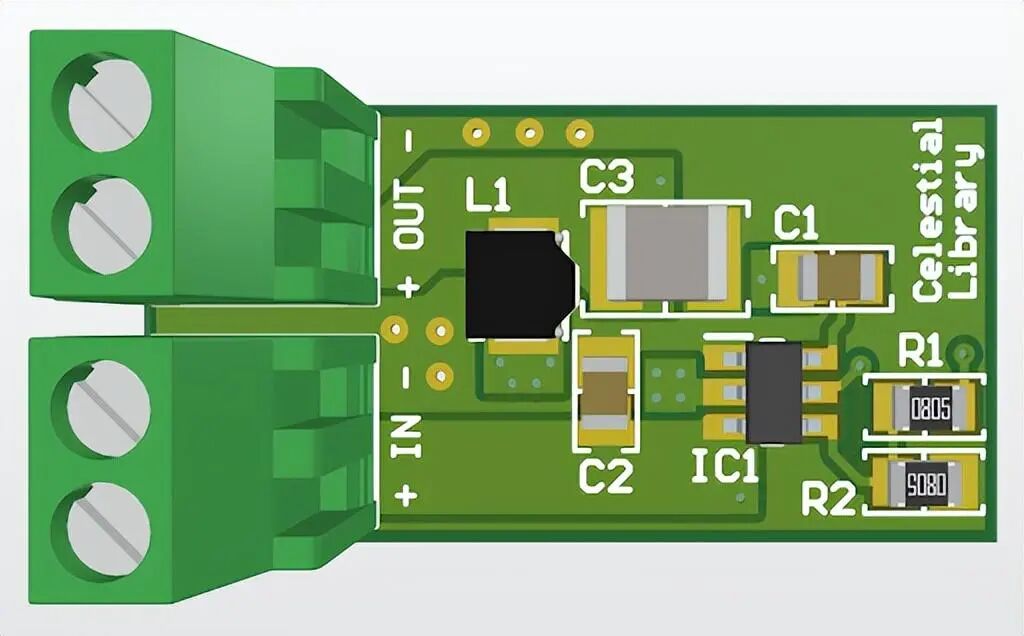
3D view of the improved PCB layout for the buck regulator
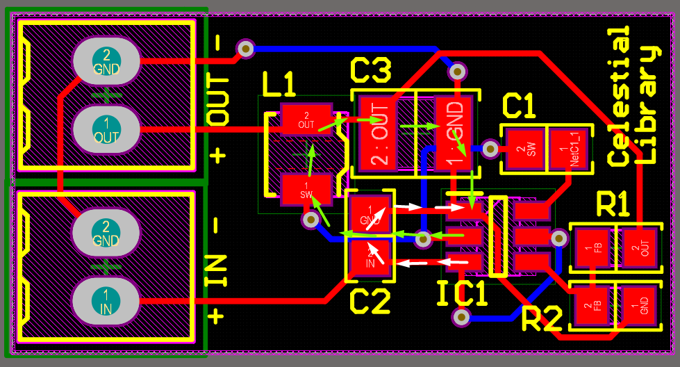
After improving the PCB layout, the output current loop is smaller, and the input and output current loops are oriented in the same direction.
5. PCB Design Summary
When designing a variable output voltage regulator schematic, careful selection of the output voltage divider is necessary. A high resistance divider can improve the efficiency of the regulator at light loads, but noise may increase. Conversely, if a low resistance divider is chosen, the effect will be the opposite.
Input capacitor selection is also complex, as it must consider input power supply voltage ripple and noise, as well as the regulator’s requirements. Additionally, the input capacitor can affect the conducted noise level on the power supply voltage, which may lead to EMC certification failures if conducted into the cables.
Inductors on switching mode regulators are also very important, ensuring they do not saturate and can operate efficiently. The type and parameters of the output capacitor will affect the conducted noise on the output voltage rail.
PCB layout is also crucial for buck converters; the current loop traces should be as short and wide as possible, ensuring that both pins of the input and output capacitors have a simple return path to the regulator. The current loops should be short, circular, and flow in the same direction to reduce EMI.
 END
END
Disclaimer:This article is reprinted from the internet, and the copyright belongs to the original author. If there are any copyright issues, please contact us in a timely manner. Thank you!