This article serves as a basic understanding and procedural reference for firmware extraction knowledge. The content mentioned will be supplemented in separate articles later.
0X01 Introduction
This article mainly focuses on firmware extraction. With the increasing number of attacks targeting devices, many manufacturers no longer provide firmware downloads, so sometimes the only way to extract firmware is through physical means from the device.
0X02 Chip Introduction
ROM Chip
Common IoT products generally use embedded Linux systems for development. One of the main purposes of chip analysis is to obtain the firmware of the hardware system and analyze potential security risks from the firmware.Firmware is generally stored in ROM, which stands for Read-Only Memory, a type of solid-state semiconductor storage that can only read the data stored in it beforehand.Its characteristic is that once the data is stored, it cannot be changed or deleted.It is usually used in electronic or computer systems that do not require frequent data changes, and the data will not disappear when the power is turned off.Common storage chips can be classified based on different reading methods and manufacturing processes into:ROM, PROM, EPROM, EEPROM, FLASH-ROM.Most IoT products use flash chips as memory, and firmware extraction is mainly done by reading flash chips.
Flash Chip
FLASH ROM is a true single-voltage chip, and its usage is very similar to EEPROM. Therefore, some books refer to FLASH ROM as a type of EEPROM.In fact, there are still differences between the two.When erasing FLASH ROM, a specific refresh program must be executed, but when deleting data, it is not done byte by byte but rather by sector (also called block) as the minimum unit, with the size of the sector varying by manufacturer;Only during writing is it written byte by byte;The read and write operations of FLASH ROM chips are performed under a single voltage, without needing jumpers, and can easily modify their content using a dedicated program;FLASH ROM generally has a storage capacity greater than EEPROM, ranging from 512K to 8M KBits. Due to mass production, the price is also quite reasonable, making it suitable for storing program code. In recent years, it has gradually replaced EEPROM and is widely used in motherboard BIOS ROM, also being a primary target for CIH attacks.Depending on the technical method, it can be divided into:IIC EEPROM, SPI NorFlash, CFI Flash, Parallel NandFlash, SPI NandFlash, eMMC Flash, USF2.0, etc.Among them, SPI NorFlash is popular due to its simple interface, fewer pins required, ease of connection, and convenient operation, and it can run code directly on the chip. Its stability is outstanding, with a high transmission rate, and it has a high cost-performance ratio when in small capacities, making it very suitable for embedded systems as FLASH ROM, thus having a very high market share.Common models like S25FL128, MX25L1605, W25Q64 are all SPI NorFlash, and their common packages include SOP8, SOP16, WSON8, US0N8, QFN8, BGA24, etc. Below is an introduction to chip classification.
1. IIC EEPROM
IIC EEPROM uses the IIC communication protocol.The characteristics of the IIC communication protocol include:Simple two-bus lines, one serial data line (SDA), and one serial clock line (SCL);Serial half-duplex communication mode with 8-bit bidirectional data transmission, with a bit rate of up to 100Kbit/s in standard mode;A type of electrically erasable programmable read-only memory that does not lose data when power is cut off, as the chip supports single-byte erase and has a very high number of erase cycles, with a theoretical value of 1 million times for a single address bit. Common chip models include AT24C02, FM24C02, CAT24C02, etc., and their common packages include DIP8, SOP8, TSSOP8, etc.
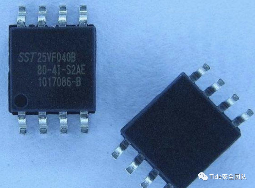
2. SPI NorFlash
SPI NorFlash uses the SPI communication protocol.It has a 4-wire (clock, two data lines, chip select line) or 3-wire (clock, two data lines) communication interface. Because it has two data lines, it can achieve full-duplex communication, making its read and write speed much faster than that of IIC communication protocol’s IIC EEPROM.SPI NorFlash has the characteristics of NOR technology Flash Memory, which allows programs and data to be stored on the same chip, with independent data and address buses, enabling fast random reads, allowing systems to read code directly from Flash;It can be programmed byte by byte, but cannot be erased byte by byte; it must erase by sector or the entire chip. Before reprogramming the memory, it needs to be pre-programmed and erased by sector or the entire chip.
NorFlash’s erase and write cycles are far below IIC EEPROM, and due to NOR technology Flash Memory’s slower erase and programming speeds and larger block sizes, the time taken for erase and programming operations is lengthy;However, SPI NorFlash has a simple interface, uses fewer pins, is easy to connect, operates conveniently, and can run code directly on the chip. Its stability is outstanding, and it has a high transmission rate, making it very suitable for embedded systems as FLASH ROM, thus having a very high market share.
Common models like S25FL128, MX25L1605, W25Q64 are all SPI NorFlash, and their common packages include SOP8, SOP16, WSON8, US0N8, QFN8, BGA24, etc.

3. Parallel NorFlash (CFI Flash)
Parallel NorFlash, also known as Parallel NorFlash, uses the Parallel interface communication protocol.It has independent data and address lines and also inherits all the characteristics of NOR technology Flash Memory;Because it uses a Parallel interface, Parallel NorFlash supports larger capacities and faster read/write speeds compared to SPI NorFlash, but due to the large number of address and data lines it occupies, it consumes many resources in electronic circuit design.Parallel NorFlash’s read/write timing is similar to SRAM, but it has fewer write cycles and is slower. Since its read timing is similar to SRAM, the read address is also linear, making it mostly used for data storage that does not require frequent changes to program code.
Common models like S29GL128, MX29GL512, SST39VF020 are all Parallel NorFlash, and their common packages include TSSOP32, TSOP48, BGA64, PLCC32, etc.
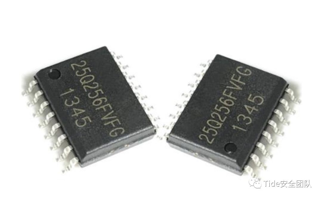
4. Parallel NandFlash
Parallel NandFlash also uses the Parallel interface communication protocol. NandFlash is categorized into three types based on process technology:SLC, MLC, TLC.
NandFlash technology Flash Memory has the following characteristics:It performs read and programming operations by page and erase operations by block;It features fast programming and fast erasing, with block erase times of 2ms, while NOR technology’s block erase times reach hundreds of ms;The chip size is small, with fewer pins, making it the lowest cost (bit cost) solid-state storage; the chip contains bad blocks, and the number depends on the memory density.Bad blocks do not affect the performance of effective blocks, but designers need to have a bad block management strategy!
Compared to Parallel NorFlash, NandFlash is faster in erasing and reading/writing, uses more erase/write cycles, and emphasizes higher performance, lower cost, smaller size, larger capacity, and longer lifespan.This makes NandFlash adept at storing pure data or files, etc., and it is widely used in embedded systems to support file systems.It is mainly used for data storage, and most USB drives use NandFlash. Currently, NandFlash is still widely used in embedded products, so measures such as bad block management and power loss protection rely on software improvements by NandFlash manufacturers.
Common models like S34ML01G100, MX30LF2G18AC, MT29F4G08ABADA are all Parallel NandFlash, and their common packages include TSOP48, BGA63, BGA107, BGA137, etc.
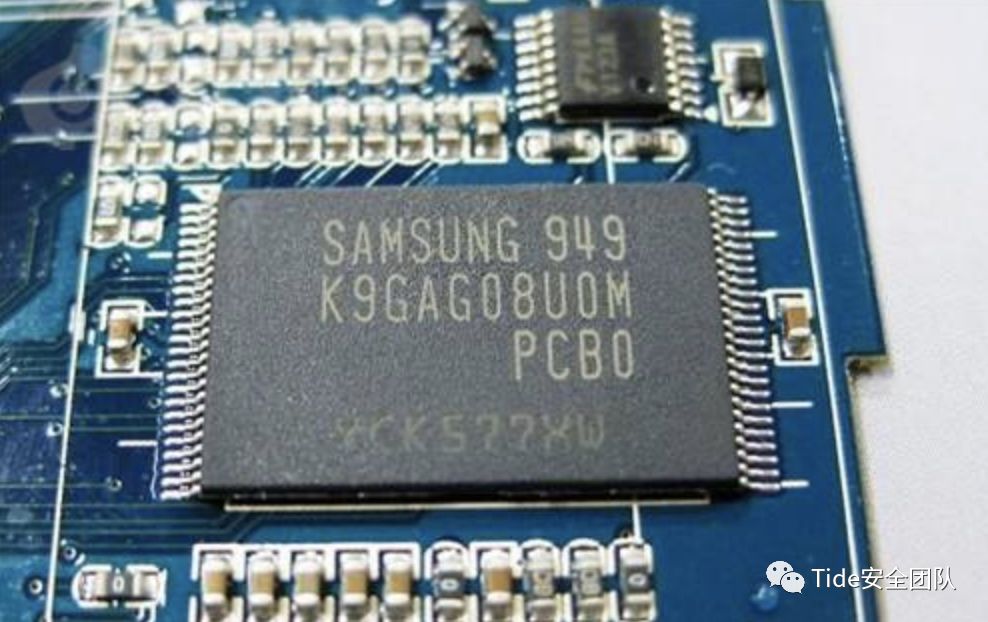
5. SPI NandFlash
SPI NandFlash uses the same SPI communication protocol as SPI NorFlash. There is no difference in read/write speed, but it adopts the same storage structure as Parallel NandFlash, so SPI NandFlash has the advantage of more erase cycles and faster erase speeds compared to SPI NorFlash. However, it will also encounter bad blocks during use, similar to Parallel NandFlash, so special bad block handling is required for use.
Another important feature of SPI NandFlash compared to Parallel NandFlash is that the chip has an internal ECC error correction module, so users do not need to use ECC algorithms for error correction calculations, allowing for simplified code and easier operations in system applications.
Common models like W25N01GVZEIG, GD5F4GQ4UBYIG, F50L1G41A are all SPI NandFlash, and their common packages include QFN8, BGA24, etc.
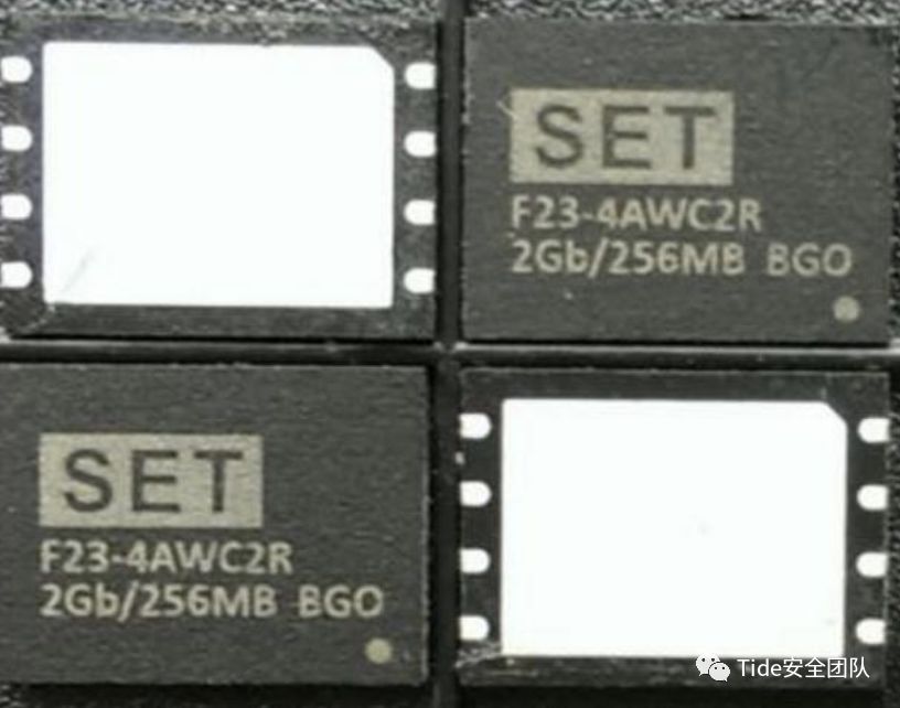
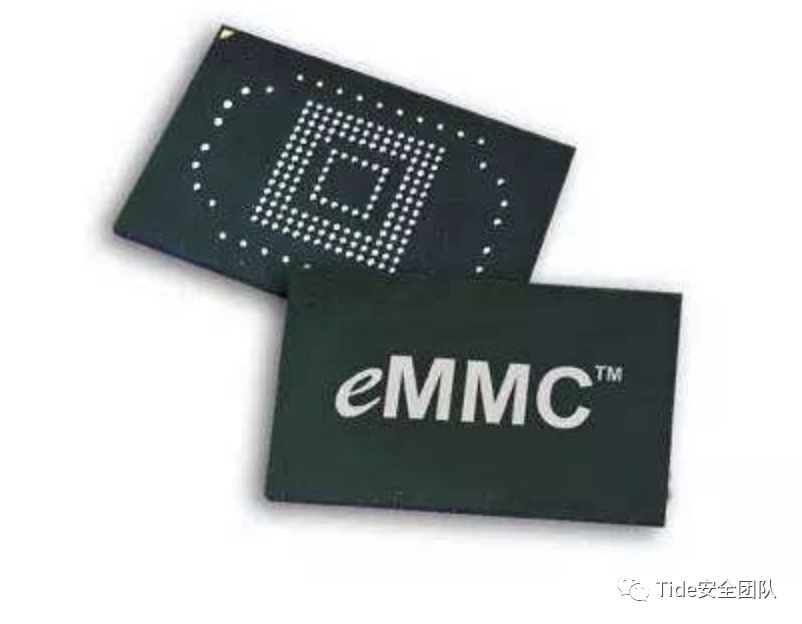
6. eMMC Flash
eMMC adopts a unified MMC standard interface, integrating an MMC Controller, with storage cells identical to NandFlash.Considering the characteristics of Flash, eMMC products internally include Flash management technologies such as error detection and correction, average Flash erase, bad block management, and power loss protection.The MMC interface speed can reach up to 52MBytes per second, and eMMC features fast and upgradable performance, with its interface voltage being either 1.8v or 3.3v.
eMMC is equivalent to NandFlash + main control IC, with an external interface protocol similar to SD and TF cards, primarily serving as the embedded storage standard for products like mobile phones or tablets.A significant advantage of eMMC is that it integrates a controller within the package, providing a standard interface and managing the flash memory, allowing mobile phone manufacturers to focus on other parts of product development and shorten the time to market.These characteristics are also important for NAND suppliers looking to reduce costs and shrink lithography sizes.
eMMC consists of an embedded storage solution with an MMC (MultiMediaCard) interface, flash storage device (NandFlash), and main controller, all in a compact BGA package, with the most common being BGA153 packaging. Common models like KLMAG8DEDD, THGBMAG8B4JBAIM, EMMC04G-S100 are all eMMC Flash.eMMC Flash has a large storage capacity, with 32GByte capacities being common in the market, and its common packages include BGA153, BGA169, BGA100, etc.
7. USF 2.0
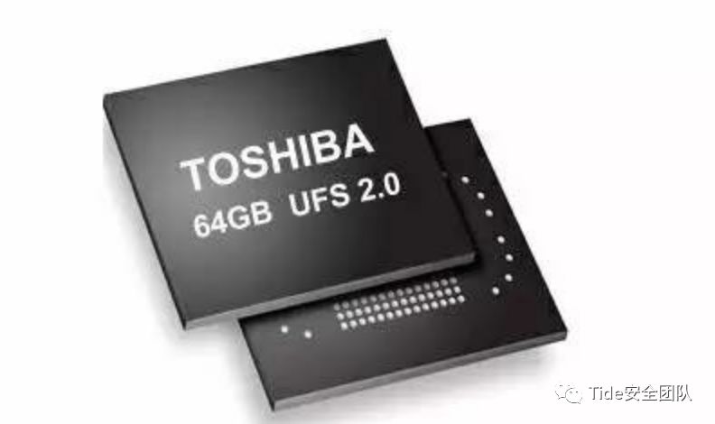
In September 2013, JEDEC released a new generation of universal flash memory standard USF 2.0, under which the flash read/write speed can reach up to 1400MB per second, which is equivalent to reading and writing the data of two CD discs in two seconds. This not only provides a significant advantage over eMMC but also makes it pale in comparison to the flash storage media solid-state drives used in computers. The UFS flash specification adopts the new standard 2.0 interface, using a serial interface similar to PATA, SATA conversion, and supports full-duplex operation, allowing simultaneous read and write operations, and also supports command queuing. In contrast, eMMC is half-duplex, where read and write must be executed separately, and commands are packaged, making it slightly inferior in speed. Moreover, UFS chips not only have fast transmission speeds but also have half the power consumption compared to eMMC 5.0, making it an ideal match for flagship mobile phone flash in the future. Currently, only a few semiconductor manufacturers provide packaged products, such as Samsung and Toshiba Electronics.
0X03 Extracting Firmware from Flash Chips
The common methods for reading the contents of Flash chips generally include the following two methods (some experts have proposed 10 methods for firmware acquisition; those interested can refer to the link numbered 3 in the reference materials):
1. Directly connect wires to the pins of the chip and connect the programmer through flying wires to read firmware online.
2. Desolder the chip and use a programming socket to read firmware offline.
1. Physical Environment
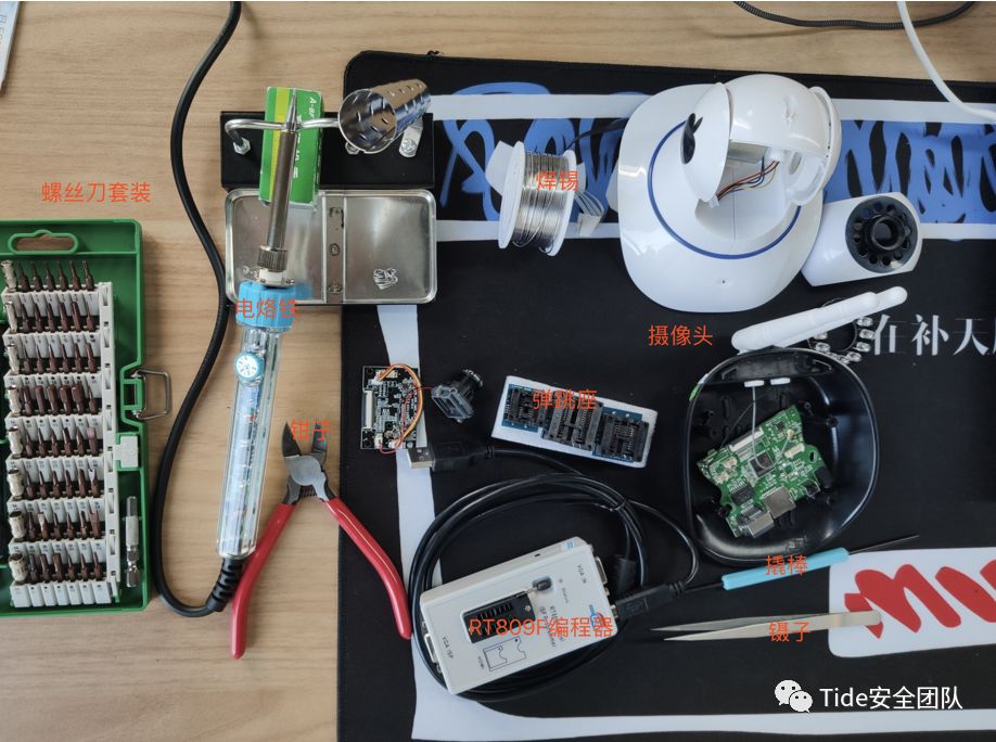
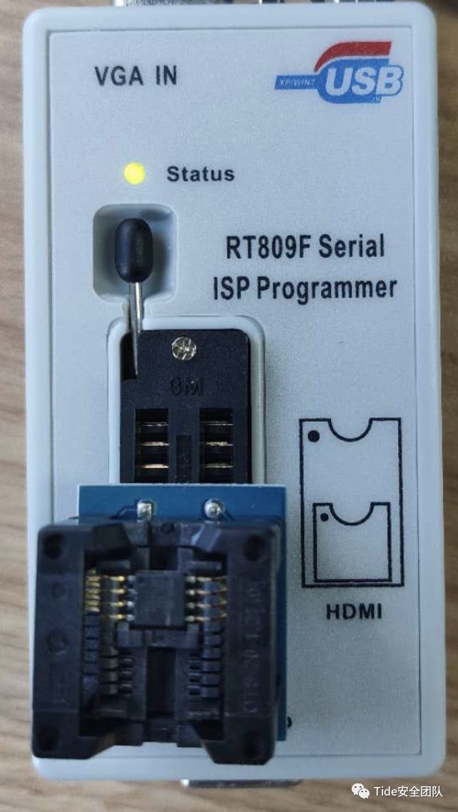
Due to a sudden interest, the tools prepared were not very sufficient, and I did not purchase chip clips, programming clips, breadboards, Dupont wires, etc. Therefore, I used the second method mentioned above, using tools to extract firmware from the camera’s 8-pin storage chip for offline programming extraction, as shown in the following image.1. RT809F Programmer2. Bounce Socket3. Soldering Iron and Tin, etc.4. Camera5. Pliers, Screwdrivers, Tweezers, Pry Bars, and other tools
2. Tool Environment
binwalk — analyzes files and file systems through firmware file headersfile — used to check if it is a valid file and file typehexdump — hex export toolstrings — similar to hexdump but can display in a readable formatdd — excavates data from binary fileslzma — decompresses LZMA files
3. Chip Extraction
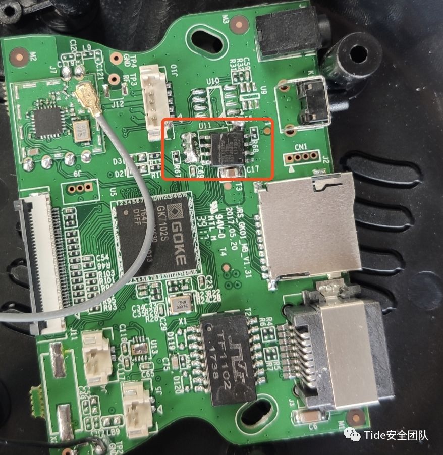
First, we use a screwdriver, pliers, and other tools to disassemble the camera housing and locate the Flash chip.
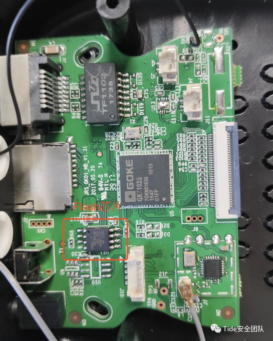
Typically, firmware is read by connecting clips to each pin and connecting them to the programmer for direct firmware reading. However, due to the lack of suitable tools, I opted to disassemble the Flash chip for firmware reading.
1. Heat the soldering iron and apply solder to one side of the chip, then gently lift that side with tweezers.
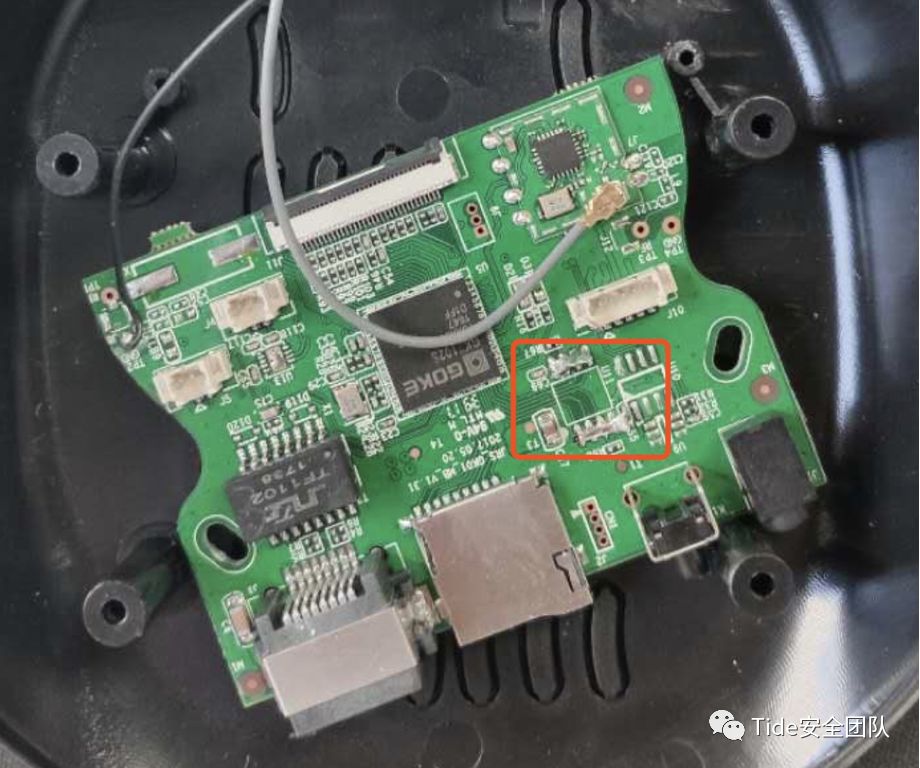
2. Apply solder to the other side of the chip, then gently lift that side with tweezers and carefully remove it.
3. Clean the solder and place the cleaned Flash chip in the bounce socket.
4. Connecting the Chip
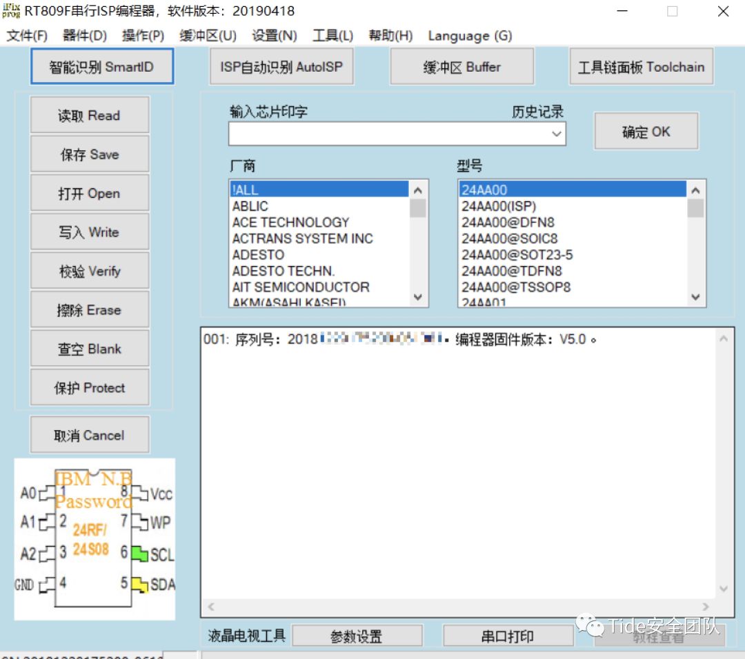
Use a USB cable to connect the programmer to the computer and open the programmer software, as shown:
5. Identifying the Chip
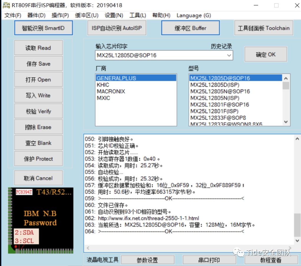
Click on Smart ID for automatic identification of the manufacturer’s chip.
6. Extracting Firmware
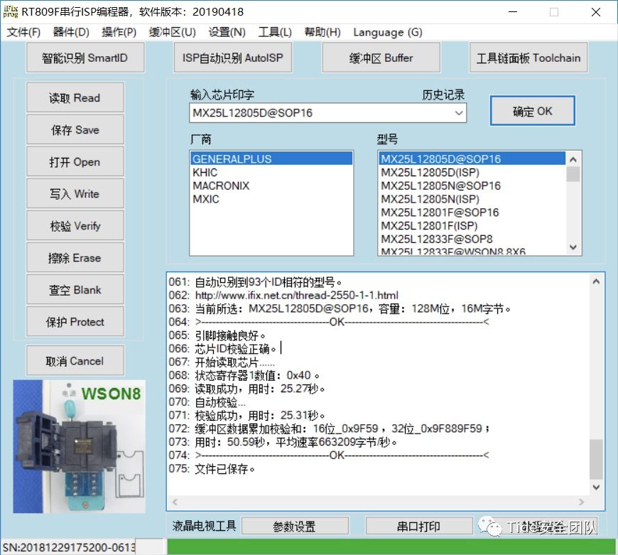
Save the extracted firmware with the .BIN suffix; thus, the firmware reading is complete, providing a foundation for the next step of firmware analysis.
0X04 Firmware Analysis
This firmware analysis serves only as a simple procedural introduction; it will be extracted and published as a separate article later.
The file command is used to check if it is a valid file and file type. The result of the file analysis can tell us whether the file is of a known type; here we can see that it only displays as a data file.

The hexdump tool allows you to analyze every byte in the file, which is very valuable. Use hexdump to analyze the firmware as follows, writing the results to a file for easier analysis:

The string command can display all printable data in the file, again writing the results to a file for easier analysis:

Binwalk analyzes binary files for possible firmware headers or file systems, then outputs each identified part along with the corresponding offset. The -e parameter automatically extracts all files from the firmware image:

0X04 Firmware Protection for Flash Chips
To prevent the firmware from being easily extracted from Flash chips, the following are recommended measures related to firmware protection:
1. For preventing firmware extraction, for MCU internal Flash, set the flash area to read protection status through programming; while external Flash firmware can generally be read.
2. For external Flash, it can be protected through circuit design, designing online detection circuits that immediately perform strong electrical attacks to destroy the Flash chip when a disconnection of the Flash chip’s pins is detected.
Original Source: Tide Security Team