It is common to see beginners of MSP430 asking questions about connecting MSP430 JTAG to the target board in forums. Here, I summarize the information to help new MSP430 learners clear their doubts.
The JTAG connection of MSP430 mainly has two methods: the 4-wire JTAG method (including TDO, TDI, TMS, TCK four standard JTAG signals) and the 2-wire Spy-Bi-Wire method (including SBWTDIO, SBWTCK two signals).
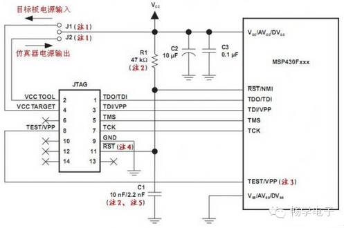
The 4-wire JTAG connection method is as follows:
Note the following points:
Note 1: You can short the J1 jumper (using the target board power supply) or short the J2 jumper (using the emulator to supply power to the target board). (Note that the J1 and J2 jumpers should be located on the user’s target board, and the user should set these two jumpers to switch the power supply method when designing the MSP430 system board.)
Note 2: The R1/C1 of the RST/NMI pin must be configured according to different device families. For detailed parameters, please refer to the recommended configurations in the MSP430 Family User’s Guide.
Note 3: The TEST/VPP pin is only available on MSP430 family devices that multiplex JTAG pins. Please refer to the specific device datasheet to determine if this pin is available.
Note 4: When the MSP430 device only has a 4-wire JTAG simulation method, the RST/NMI pin in the JTAG connector is optional; it can be used or not used, as this signal is not needed during device programming and simulation. However, when using the 4-wire JTAG simulation method on devices with a 2-wire Spy-Bi-Wire simulation interface, the RST/NMI signal must be connected.
Note 5: When using the 4-wire JTAG simulation method on devices with a 2-wire Spy-Bi-Wire simulation interface, the maximum value of the C1 capacitor must not exceed 2.2nF.
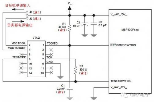
The 2-wire Spy-Bi-Wire JTAG connection method is as follows:
Note the following points:
Note 1: You can short the J1 jumper (using the target board power supply) or short the J2 jumper (using the emulator to supply power to the target board). (Note that the J1 and J2 jumpers should be located on the user’s target board, and the user should set these two jumpers to switch the power supply method when designing the MSP430 system board.)
Note 2: Be aware that the RST/NMI pin of the device is used as a bidirectional debug data communication interface in the 2-wire Spy-Bi-Wire simulation method. Therefore, the capacitor on this pin will affect the emulator’s ability to establish a simulation link with the device. When using the MSP430UIF, the maximum value of the C1 capacitor is 2.2nF.
Note 3: The purpose of resistor R2 is to protect the TCK signal of the emulator from the voltage impact of the JTAG fuse blowing during the simulation. This voltage is provided by the emulator’s TEST/VPP pin, which is about 6V. When not using the fuse-blowing function, resistor R2 can be omitted (i.e., replaced with a 0Ω resistor) and the TEST/VPP pin should not be connected to the device.
Once you are very familiar with the above two connection methods, you can simplify the power part according to your MSP430 system board without being too rigid about the above requirements.