Implementing the TAP controller within the SoC, interfacing with the JTAG chip in the JTAG hardware box to receive and process JTAG sequences. Its main structure is as follows: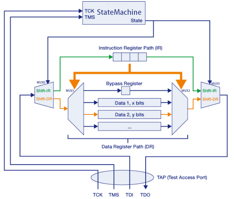 As can be seen, there is a state machine, an Instruction Register (IR), several Data Registers (DR), a Bypass Register, etc.The state machine is controlled by TMS, and the state machine outputs State to control MUX0/3: either Shift-IR or Shift-DR. If it is Shift-IR, the bit stream from TDI enters the IR, while the IR controls the MUX1/2 selector: outputting the Bypass Register, or whichever DR register, etc. The contents of the IR or DR are output from TDO.A complex SoC may have multiple TAPs, which form a TAP network, as shown in the diagram below:
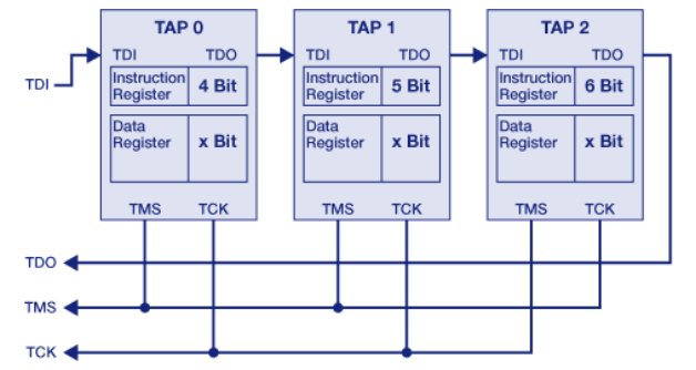 This diagram reveals that TCK and TMS simultaneously act on each TAP controller, while the TDO output of one TAP connects to the TDI input of the next TAP, and each TAP has different internal IR or DR. This is one of the reasons why each SoC’s JTAG debugging has independent configurations.The TAP network composed of multiple TAPs may have one TAP that serves as the entry point for another complex SoC partition. Therefore, when JTAG needs to enter that partition, it must send the correct JTAG sequence, such as selecting or enabling that TAP while allowing other TAPs to Bypass or Disable, depending on the specific implementation of each SoC.