
The inference scenarios of algorithm solidification and large-scale deployment are eroding the market originally belonging to GPUs. ASIC chips, with their extreme energy efficiency and low-cost advantages, have become the new favorites of tech giants.
By 2025, global tech giants will face a common challenge: how to efficiently handle the explosive growth of artificial intelligence inference computing demand. With the popularization of large model applications like ChatGPT, inference computing has accounted for over 70% of total AI computing demand, which is 4.5 times that of training demand.
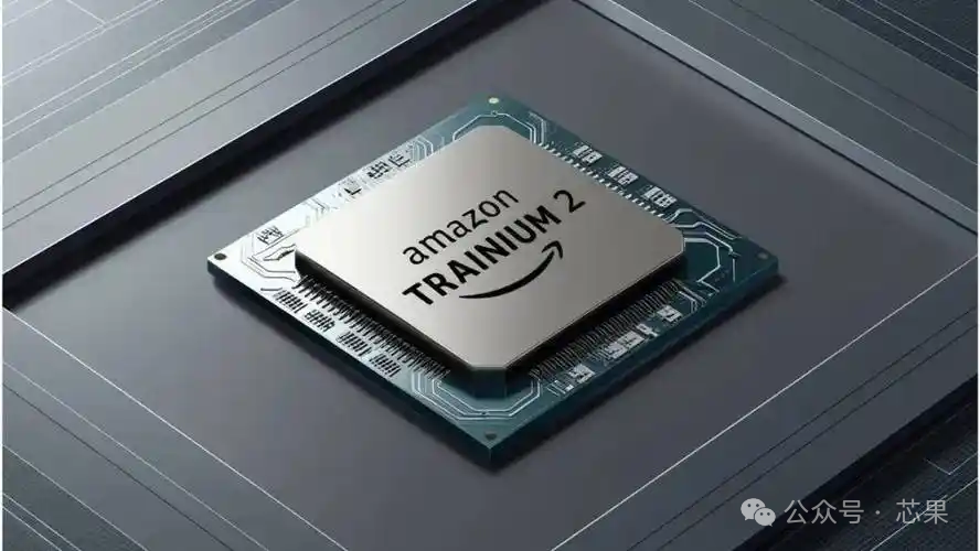
Google’s latest generation TPU is deeply optimized for the Transformer architecture, achieving over 30% improvement in computing efficiency compared to the previous generation; Amazon AWS’s Trainium 2 focuses on distributed training scenarios, supporting parallel computing for models with hundreds of billions of parameters.
In specific scenarios, the performance of these ASICs has approached or even surpassed that of NVIDIA’s A100 GPU.
01 Market Explosion: From Scale Forecast to Demand-Driven
The ASIC market is experiencing explosive growth. Marvell revised its global ASIC market size forecast for 2028 at the Custom AI Investor Event, raising it by 29% from $42.9 billion to $55.4 billion.
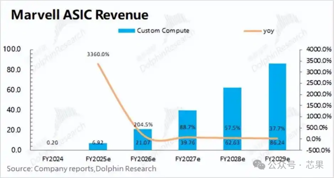
Minsheng Securities pointed out that the global ASIC trend is accelerating, and custom chips are entering a golden development period. In terms of compound growth rate, the ASIC market size in 2023 is about $6.6 billion, and it is expected to reach $55.4 billion by 2028, with a compound annual growth rate of 53%. The explosive growth of inference demand at the application end is the main driving force. Major companies are simultaneously increasing investment in custom ASIC chips to reduce costs and stabilize supply.
Tech giants like Google and Meta are increasing their investment in self-developed ASIC chips, all aimed at addressing the explosive growth of AI inference computing. The urgent demand from cloud service providers for “cost reduction and efficiency improvement” is driving the popularity of ASICs. Google processes billions of search requests daily, AWS supports the cloud computing needs of millions of enterprises worldwide, and Meta’s social platform generates massive interaction data every second. The AI tasks in these scenarios are relatively fixed, perfectly matching the core advantage of ASIC’s “customization”.
02 Performance Advantages: How ASIC Surpasses GPU
ASICs have shown significant advantages in the inference field. Especially in scenarios of algorithm solidification and large-scale deployment, ASICs are eroding the market share originally held by GPUs due to their extreme energy efficiency and low costs.
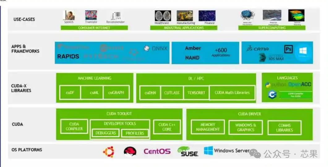
Energy efficiency is the core advantage of ASICs. The energy efficiency ratio of Google’s TPU v5e is three times that of NVIDIA’s H100, and AWS Trainium has a cost-performance ratio that is 30%-40% higher than H100 in inference tasks. This advantage stems from ASIC’s “extreme adaptation” to specific algorithms.
Once a model is deployed, its algorithm logic and computing processes will be fixed for a long time. ASICs can directly “solidify” these logics into the hardware architecture, eliminating redundant modules used for general computing in GPUs, allowing hardware resources to serve the target task 100%.
The cost advantage is also significant. An NVIDIA GPU consumes about 700 watts, with an hourly electricity cost of about 0.56 yuan when running large models; while an ASIC chip with equivalent computing power can control its power consumption within 200 watts, with the same task costing only 0.16 yuan per hour.
For applications requiring hundreds of thousands of inference chips, this difference translates to annual cost savings of hundreds of millions.
03 Major Players’ Layout: The ASIC Strategy of Tech Giants
Global tech giants are increasing their investment in ASICs to capture the computing power dividends of the AI era. Google continues to iterate its self-developed TPU for large model inference; Amazon has launched the Trainium chip to optimize training performance; Meta and Microsoft are also accelerating the layout of their own AI chip systems.
Google was one of the first companies among CSPs to develop its own ASIC chips, with its TPU series dating back to the V14 launched in 2015. In 2023, Google showcased the TPU V4 at the Hot Chips conference and achieved mass production; in April 2025, it will release the latest TPU V7, significantly improving performance.
Amazon’s Chandler chip is designed for AWS’s AI training and inference. Training 2 has entered a cabinet form connected to sky up, with performance increasing fourfold compared to the previous generation. In terms of network architecture, 16 chips inside the server use a 4×4 or 2×2×2×2 hypercube grid.
Meta’s self-developed chip was released later, but it is advancing rapidly in research and market deployment by 2025. The latest product is the V2 released in 2024, with a process upgrade from 7nm to 5nm, and interconnect technology upgraded to PCIe 5.0, with plans for the next generation to upgrade to 3nm.
In terms of shipment volume, Google’s self-developed TPU chip is expected to reach 1.5 to 2 million units by 2025, while Amazon AWS’s Trainium 2 ASIC is about 1.4 to 1.5 million units, with the combined scale approaching 40%-60% of NVIDIA’s AI GPU during the same period.
04 Ecosystem: The Industrial Chain Pattern from Design to Manufacturing
The ASIC industrial chain covers all aspects from chip design, manufacturing to packaging. Broadcom and Marvell are leaders in the global ASIC design service field, with Broadcom accounting for about 60% of the market share, while Marvell accounts for about 10%.
Broadcom is closely tied to top companies like Google and Meta. In 2019, AI business accounted for about 5% of Broadcom’s revenue, which increased to 15% in 2023, with AI business revenue exceeding guidance at $12.2 billion for the 2024 fiscal year.
In the latest fiscal quarter, AI-related revenue grew by 46% year-on-year, accounting for over 50% of semiconductor revenue, becoming a core growth engine.
Marvell is gradually taking over some of Broadcom’s business in AWS products. In Q1 2026 (ending July), revenue growth rate exceeded 60% (a record high), with data center business accounting for 75%.
The company has raised its market space forecast for data center business in 2028 from the original upper limit of $75 billion to $94 billion, with AI accelerator business accounting for over 60%.
Chip foundry giants like TSMC and Samsung have also begun collaborating with customers to develop ASIC projects. TSMC’s CoWoS packaging technology is a key link in the mass production of ASIC chips, but currently, CoWoS wafer capacity can only support 300,000-400,000 pieces, far below Meta’s target of 1 million-1.5 million units.
In China, driven by both policy and capital, the AI ASIC market is expected to enter a period of rapid expansion. SMIC, as a leading global integrated circuit foundry, currently has wafer capacity in a tight supply-demand situation, and will benefit from the incremental business brought by the development of domestic AI ASICs.
05 Domestic Opportunities: The Development Prospects of China’s ASIC Industry
The Chinese ASIC industry is ushering in development opportunities under domestic substitution and policy support. Under U.S. export controls, the market share of Chinese ASIC companies is expected to rise from less than 20% in 2024 to 40% in 2025.
Huawei’s Ascend 910B achieves a computing power density of 2.5 PetaFLOPS through Chiplet technology and has been connected to the National Supercomputing Center in Guangzhou. Zhonghao Xinying’s “Moment” TPU adopts a storage-computing integrated architecture, achieving an energy efficiency ratio of 30 TOPS/W, surpassing NVIDIA’s A100’s 20 TOPS/W.
In terms of policy support, the “East Data West Computing” project has driven a surge in ASIC demand for data centers in the west, with over 500,000 domestic AI chips deployed in the Ningxia hub cluster.
The National Integrated Circuit Fund’s third phase has invested over 200 billion yuan, establishing an advanced ASIC packaging testing center in Zhangjiang, Shanghai, to tackle key processes such as CoWoS and TSV.
Many domestic companies are expected to benefit from the wave of ASIC development. Placo New Material’s chip inductors can be applied to ASIC chips, providing power supply for their front end, and feature miniaturization and high current resistance.
Guokai Micro’s AI edge computing chip is developed based on the underlying architecture design of large models, and is compatible with traditional CNN architectures, thus achieving high energy efficiency.
Aojie Technology has a chip customization team of about 400 people, which not only assists in its own 4G/5G baseband chip development but also undertakes external projects. It has accumulated self-developed IP in the mobile chip field, with some IP already licensed for use by mobile manufacturers.
The company’s advanced process chips have the capability of successful mass production in one go, and progress has been made in cooperation with domestic internet companies.
06 Challenges and Limitations: Obstacles Faced by ASICs
Despite the significant advantages of ASICs, large-scale deployment is not without challenges. Behind this computing power race lie multiple challenges of capacity, technology, and risk. The capacity bottleneck is the most pressing issue. Meta’s planned mass production of the MTIA chip in 2026 relies on TSMC’s CoWoS technology, but the current CoWoS wafer capacity can only support 300,000-400,000 pieces, far below its target of 1 million-1.5 million units.
If Google, AWS, Microsoft, and other manufacturers simultaneously expand production, high-end packaging capacity will become a “bottleneck” restricting the volume of ASICs. Although TSMC plans to increase CoWoS capacity by 50% by 2025, it will take 12-18 months from capacity construction to actual production, making it difficult to alleviate supply-demand conflicts in the short term. Large-size CoWoS packaging requires high consistency in chip design and materials, with system debugging cycles lasting 6-9 months. Even for a mature technology like Google’s, a significant amount of resources must be invested to solve issues such as heat dissipation and signal interference.
A more subtle risk lies in the “specialization trap” of ASICs. AI model architectures are not static; if the future shifts from Transformers to new architectures, the ASICs invested in earlier may face the risk of becoming “instantaneously obsolete.” Jensen Huang has stated, “A perfect ASIC performs excellently in certain tasks but poorly in others. Once the AI workload changes, it becomes useless.”
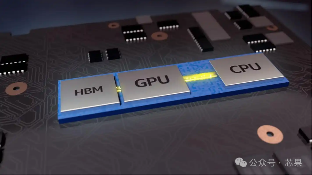
This is also why Google’s Gemini model is still deployed on NVIDIA GPUs—by using a hybrid architecture of “general + specialized” to hedge against technological iteration risks. The “butterfly effect” of the supply chain cannot be ignored either. If cloud service providers like Meta and AWS concentrate their orders, key materials such as high-end ABF substrates, HBM3E memory chips, and liquid cooling components are likely to become scarce, further driving up costs and slowing down mass production.
07 Future Trends: The Coexistence Pattern of ASICs and GPUs
The rise of ASICs does not mean the decline of GPUs; rather, it marks the beginning of a shift in the AI computing power market from “one dominant force” to “multiple symbiotic entities.” The ultimate outcome of this transformation is likely to be a dual-track parallel pattern of “general GPUs + custom ASICs.”
In the short term, ASICs are an “incremental supplement” rather than a “replacement of existing stock.” NVIDIA still holds an absolute dominance in the high-end training market (such as models with hundreds of billions of parameters), and its technological accumulation and ecological advantages are unlikely to be shaken in the short term. ASICs are rapidly penetrating specific scenarios, becoming an important choice for cloud service providers to reduce costs and improve efficiency.
2025-2026 will be a transitional period of dual-line parallelism, with the market exhibiting characteristics of “GPU-dominated value, ASIC growth quantity.” Nomura Securities predicts that the overall shipment volume of ASICs is expected to surpass NVIDIA GPUs at some point in 2026. In the long term, the market will show a “layered competition” pattern. NVIDIA will continue to lead the general AI computing power market, supporting cutting-edge model exploration and complex task processing. ASICs will occupy advantages in vertical scenarios, maximizing efficiency through customization.
From the application dimension, the division of labor between the two will become clearer: GPUs will be responsible for “innovation exploration from 0 to 1,” while ASICs will handle “scaling from 1 to N.” Just as supercomputers are used for cutting-edge scientific research, while dedicated servers support daily data processing, the AI computing power market will also form a balance of “innovation and efficiency.” Industry data also confirms this trend. Morgan Stanley predicts that the AI ASIC market size will grow from $12 billion in 2024 to $30 billion in 2027, with a compound growth rate of 34%, while the GPU market will still maintain a growth rate of over 20% during the same period.
This means that the rise of ASICs is about expanding the “cake” of the AI computing power market, rather than simply seizing GPU market share. Chip foundry giants TSMC and Samsung have already begun collaborating with customers to develop ASIC projects, while traditional chip companies like Broadcom and Marvell have repeatedly emphasized their commitment to expanding their presence in the AI chip field. However, high-end packaging capacity remains a “bottleneck” restricting the volume of ASICs. Although TSMC plans to increase CoWoS capacity by 50% by 2025, it will take 12-18 months from capacity construction to actual production, making it difficult to alleviate supply-demand conflicts in the short term.
The future AI computing power market will not be a zero-sum game of “either/or,” but rather a symbiotic ecosystem where each has its strengths. NVIDIA will continue to dominate the general computing power market with its technological, ecological, and supply chain advantages. Giants like Google, AWS, and Meta will build barriers in vertical scenarios through ASICs; while companies like Broadcom and Marvell will also share a piece of the pie in the custom chip field.