Micro Interview: Lin Feng, Deputy General Manager of Fushi Technology
Interview Background: Fushi Technology Co., Ltd. (abbreviated as Fushi Technology) has been invited to participate in the “38th ‘Micro Words and Great Meaning’ Seminar: LiDAR and 3D Sensing Technology” to be held on September 11, 2025, from 13:30 to 13:55 during the China International Optoelectronic Exposition (CIOE), where they will share a keynote speech titled “Fushi Technology’s Universal Optical Control™ Technology Drives the Implementation of Vehicle All-Solid-State Laser Main Radar.” As this seminar approaches, Maims Consulting is fortunate to interview Lin Feng, Deputy General Manager of Fushi Technology.

Lin Feng, Deputy General Manager of Fushi Technology
Company Introduction: Fushi Technology was established in 2017 and is an innovative technology enterprise focused on the design of core chips for machine vision. With a strong technical foundation, Fushi Technology continues to break through in niche areas: its 3D facial recognition chip and algorithm solution for near-range machine vision holds the largest market share in the smart lock sector; in the field of long-range machine vision, it has launched and mass-produced the industry’s first third-generation all-solid-state LiDAR (LiDAR) array SPAD-SoC laser receiving chip, providing chip-level “artificial intelligence eyes” for autonomous driving, intelligent robots, and other smart terminal fields.
Fushi Technology is recognized as a national specialized and innovative “little giant” enterprise, a national high-tech enterprise, the first completion unit of the Guangdong Provincial Science and Technology Progress Award (second prize), a member of the Guangdong Provincial Human-Machine Interaction Sensor Engineering Technology Research Center, and a member of the Hong Kong Science Park Elite Enterprise Program. The company is also undertaking three major municipal-level technical research projects related to all-solid-state LiDAR. Fushi Technology currently has one municipal-level leading talent, several high-level overseas talents, and PhDs from well-known universities, with a core team that has over 20 years of experience in the chip industry. The chips designed by the team in various fields have achieved the number one market share, with historical cumulative shipments reaching billions of units.
Maims Consulting: Hello, Mr. Lin, thank you for accepting the interview with Maims Consulting. First, please introduce yourself (educational and work experience), and then explain your responsibilities at Fushi Technology.
Lin Feng: I studied microelectronics and integrated circuit design. For the past 20 years after graduation, I have been engaged in the design and mass production of mixed-signal chips in the semiconductor industry. Over the years, I have participated in the R&D and mass production of various LCD and OLED display driver chips, electronic paper driver chips, fingerprint recognition chips, and single-photon avalanche diode (SPAD) chips for direct time-of-flight (dToF).
Maims Consulting: Fushi Technology has experienced rapid growth from technology R&D to product implementation in nearly eight years since its establishment. Could you review the company’s important milestone events and their impact on the company’s development?
Lin Feng: Fushi Technology was established in 2017, leveraging the team’s over ten years of chip design experience in the mobile phone industry to fully invest in the R&D and mass production of key chips in the machine vision field. In 2019, our near-range 3D machine vision products successfully opened the 3D facial recognition market, and then we challenged the more difficult long-range dToF LiDAR field by developing SPAD device chips. To achieve cost-effective long-range 3D machine vision, we assembled a technical team for SPAD chips both domestically and internationally, focusing on recruiting several high-level overseas talents and returning PhDs. We built a SPAD chip technology system based on the underlying theory of semiconductor process devices and LiDAR systems, investing heavily in R&D funds for engineering wafer production testing to validate chip design theories and device parameters, working day and night to solve technical challenges. In the R&D of SPAD chips, the company has invested over 300 million yuan in R&D funds. After accumulating experience from the R&D and mass production applications of the first-generation single-point LiDAR and second-generation line-array LiDAR chips, we successfully completed the third-generation array SPAD wafer tape-out in June 2023, and within a month, we completed the engineering prototype, releasing the first domestic SPAD-SoC large-array all-solid-state LiDAR chip in August. This has established Fushi Technology’s leading position in the domestic all-solid-state LiDAR SPAD-SoC chip field.
Maims Consulting: How does Fushi Technology stand out in SPAD-SoC chip design and LiDAR algorithm capabilities? Please elaborate. What arrangements has Fushi Technology made regarding core patents?
Lin Feng: The technology accumulation of Fushi Technology’s SPAD-SoC chip has not been achieved overnight. Since 2019, we have been developing SPAD chips, maintaining a rhythm of developing and mass-producing one SPAD chip each year, starting from single-point near-range LiDAR chips. We have accumulated experience in different requirements such as 4-meter, 15-meter, and 30-meter ranging, continuously applying mass production in various terminal products such as sweeping robots, drones, intelligent AGV unmanned vehicles, and AR/VR glasses based on consumer and industrial application scenarios, obtaining first-hand practical testing data. Based on our own SPAD chip foundation, we have accumulated the most fundamental data, continuously iterating our LiDAR algorithm capabilities, and forming proprietary intellectual property rights for the optimized algorithms as a LiDAR DSP algorithm module embedded in the SPAD-SoC chip. Ultimately, the large-array SPAD-SoC chip has achieved the highest resolution performance of all-solid-state LiDAR, with a laser processing speed of 540,000 points per second, achieving the best cost-performance ratio in terms of processing speed, chip area, and processing power consumption. During the R&D process, Fushi Technology has comprehensively laid out over 160 invention patents for SPAD chips and all-solid-state laser emission module materials and optical designs both domestically and internationally, covering key components of all-solid-state LiDAR emission and reception, ensuring that Fushi Technology’s customers can obtain sufficient intellectual property protection for their product sales globally.
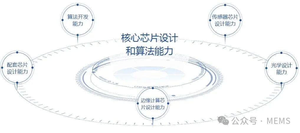
Core chip design and algorithm capabilities of Fushi Technology
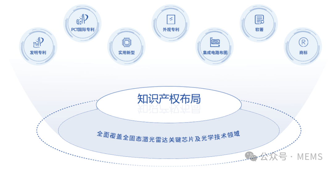
Intellectual property layout of Fushi Technology
Maims Consulting: What is the current progress of Fushi Technology’s core LiDAR chip? What are the core product technical advantages and market prospects?
Lin Feng: Based on years of experience with SPAD chips, when developing the large-array SPAD-SoC chip for LiDAR, we began designing with consideration of the entire LiDAR emission and reception system. We also designed supporting laser driver chips and laser emission VCSEL chips. After the large-array SPAD-SoC wafers were produced, we quickly achieved engineering prototypes within a month, delivering them to customers for testing. After years of customer application testing and feedback, we have accumulated supporting solutions for various application scenarios. In the new generation of all-solid-state LiDAR, the large-array SPAD-SoC chip we launched has been adopted by multiple LiDAR customers, making us one of the few suppliers capable of providing a complete set of key chips for all-solid-state LiDAR at mass production levels. Customers can quickly integrate existing mature solutions and achieve mass production. Additionally, many system integrators in the intelligent industry are adopting Fushi Technology’s SPAD-SoC chips, embedding LiDAR functionality into their own system products, becoming an important part of their systems, entering various industries such as unmanned vehicles, lawn mowers, smart engineering, smart construction sites, and security monitoring. The all-solid-state LiDAR using SPAD-SoC chips is compact, cost-effective, high-resolution, and highly reliable, capable of flexibly adapting to most AI scenarios for autonomous movement or fixed-point use. End users can also develop intelligent algorithms based on the open data from the LiDAR chip for their required application scenarios. We believe that by further optimizing the technology of the laser emission module, reducing costs, and increasing ranging distances, the application coverage of all-solid-state LiDAR will become even broader.
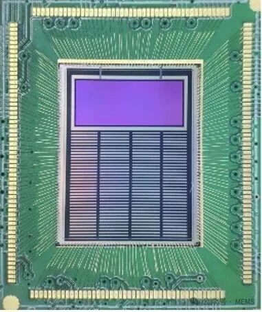
Fushi Technology’s large-array SPAD-SoC chip
Maims Consulting: In July 2025, a well-known automotive company publicly released its latest intelligent driving assistance platform, equipped with five LiDAR solutions, four of which use Fushi Technology’s large-array SPAD photodetector chip solution (360 x 150 pixel array). Please introduce the special designs made by this chip to meet automotive-grade requirements. What were the most challenging aspects of collaborating with the automotive company?
Lin Feng: Automotive LiDAR presents significant challenges, requiring high environmental adaptability and chip reliability, while blind-spot radar must consider compact size and thermal balance, all adhering to the industry’s highest standards. Fushi Technology’s large-array SPAD-SoC chip was designed with targeted considerations from the outset, featuring a large-resolution photodetector surface of 360 x 150 pixels, which meets the needs of automotive angular radar to cover a wide field of view (FoV) detection. The automotive company achieved a large detection area coverage of 150° x 112° through a dedicated lens. Additionally, through extensive testing in various environmental settings, we continuously upgraded the LiDAR signal algorithms to adapt to environmental noise, improving the signal-to-noise ratio and ranging accuracy. Based on accurate spatial environmental detection data, the automotive company utilized its robust driving assistance algorithms to easily handle extreme environmental tests such as parking next to stairs in complete darkness. By equipping four all-solid-state LiDARs, the vehicle can achieve 360° real-time environmental detection, ensuring safe distance control from surrounding objects during steering or automatic parking, thus enabling high safety operations.
Maims Consulting: From completing samples to achieving mass production, there are numerous challenges in quality control and reliability assurance. What measures and management systems does Fushi Technology have in place for this?
Lin Feng: The team at Fushi Technology has extensive experience in the mass production of chips, holding high standards for product reliability. Several years ago, we introduced TUV Rheinland for training and consulting on automotive product systems and safety requirements. Currently, within the company, products are designed and produced according to automotive product design and production requirements, achieving controllable and traceable standard audits at every stage of the process, having undergone audits from multiple automotive manufacturers. Fushi Technology strictly adheres to customer requirements, conducting automotive-grade testing and certification for chips to ensure compliance with the supply quality system requirements for automotive-grade chip products.
Maims Consulting: What do you believe are the key development trends for SPAD technology in the coming years? What directions will Fushi Technology focus on in these trends? Besides automotive LiDAR, in which other fields will Fushi Technology’s SPAD technology be applied?
Lin Feng: SPAD chips are among the most imaginative products in the commercial realm of photodetector chips in recent years. Due to their complete compatibility with silicon-based CMOS process lines, they can integrate the laser reception circuit system that previously required hundreds of complex separate device chips onto a single chip, truly achieving integration of sensing, storage, and computation. This greatly reduces the cost and size of LiDAR while significantly enhancing the overall system reliability. Moreover, the large-area photodetector integration of SPAD chips can directly cover the entire space, eliminating the need for beam deflection devices (such as rotating mirrors or MEMS scanning mirrors) for laser scanning. Therefore, all-solid-state LiDAR based on SPAD chips has become the main direction for the generational evolution of LiDAR.
As one of the first companies in China to mass-produce large-array SPAD-SoC chips, Fushi Technology will focus on key technical challenges in the development of all-solid-state LiDAR chips. LiDAR is a system of light emission and reception. Fushi Technology has already resolved most of the technical issues related to SPAD-SoC light reception chips. Next, we will focus on the world-class technical challenges of high-power laser emission scanning required for all-solid-state LiDAR, aiming to advance the successfully developed all-solid-state optical deflection technology—Universal Optical Control™—to mass production, filling the last gap in the technology segment of all-solid-state LiDAR. We believe that in the near future, everyone will soon see the finished product of all-solid-state long-distance LiDAR, further enhancing the product capabilities of LiDAR and penetrating various industries. Only by expanding the application scenarios of LiDAR can we drive the collaborative development of the industry chain, jointly enlarging market increments and achieving a win-win situation for all parties.
Maims Consulting: Compared to international leading companies (such as Sony) in SPAD technology, where do you think domestic companies fall short in design, manufacturing, packaging, and testing along the industrial chain? How can these gaps be narrowed?
Lin Feng: Sony is one of the earliest companies to develop SPAD photodetector chips. With its own wafer fab, it maintains a leading position in SPAD process development, and its SPAD performance parameters are industry-leading. Domestic companies are continuously catching up. After years of collaboration with wafer fabs, Fushi Technology has significantly improved SPAD performance, for example, the sensitivity (PDE) parameter of SPAD in the 940 nm wavelength band has narrowed the gap from 50% in the past to about 5% now, reaching world-class levels and fully meeting the performance required for long-distance laser systems while achieving stable mass production. Additionally, all-solid-state LiDAR is a complex system that not only refers to SPAD performance but also requires signal processing circuits, time conversion circuits, control schemes for the LiDAR system, and coordination with laser emission modules to achieve a high cost-performance ratio for the entire all-solid-state LiDAR system. Domestic companies are closer to domestic customers, with a large number of new energy vehicles produced by domestic companies, and they cooperate fully among themselves to quickly iterate system requirements, forming their own technological advantages. For example, Fushi Technology’s upcoming Universal Optical Control™ all-solid-state optical module scanning technology can effectively solve the power and scanning angle challenges of laser emission modules, completing the last shortcoming of long-distance all-solid-state LiDAR over 200 meters. Combined with Fushi Technology’s SPAD-SoC chips, it can achieve truly long-distance all-solid-state LiDAR products, greatly broadening the application coverage of SPAD chips.
Maims Consulting: Looking ahead to the next five years, what key goals does Fushi Technology hope to achieve in technology and market? What plans do you have for resource integration in the industrial chain and global layout?
Lin Feng: From the very beginning, Fushi Technology positioned itself in the field of human-computer interaction technology, aiming to provide the most advanced and reliable 3D machine vision for the rapidly developing artificial intelligence. With the explosive growth of autonomous mobile intelligent devices, embodied intelligence is becoming an important industry that will impact the future of humanity. Fushi Technology has simultaneously invested in technology R&D layouts both domestically and internationally, hoping to use SPAD chips as a “retina” to integrate chip technology and optical material technology, providing the global market with a high cost-performance ratio “artificial intelligence eyes” technology combination, vigorously promoting the industrial development of embodied artificial intelligence.
Maims Consulting: In September 2025, you will participate in the “38th ‘Micro Words and Great Meaning’ Seminar: LiDAR and 3D Sensing Technology” and deliver a keynote speech. What aspects of technology sharing and communication will you bring to the audience?
Lin Feng: For a long time, whether it is mechanical rotating LiDAR or semi-solid rotating mirror LiDAR, it has been commonly perceived that there must be a rotating component to reflect laser for scanning. This has been a long-standing pain point in the LiDAR industry. Rotating components have also brought many issues within LiDAR, such as noise, time reliability, and high-precision production alignment requirements. These problems have led to high costs for LiDAR, preventing widespread application.
With the emergence of all-solid-state LiDAR, the industry has entered a new development phase. However, current all-solid-state LiDAR also faces the issue of insufficient solid-state emission power, limiting its use to short and medium distances. As one of the first companies in China to mass-produce all-solid-state LiDAR SPAD-SoC chips, Fushi Technology aims to break the “tightening spell” of laser emission power. Therefore, we began the R&D of all-solid-state optical deflection technology years ago, aiming to resolve the contradiction between “high power” and “low cost” for long-distance light emission over 200 meters, avoiding the use of rotating components such as mirrors or MEMS, ensuring that LiDAR can achieve true “all-solid-state” while meeting long-distance detection requirements. Today, Fushi Technology has finally solved all technical challenges and officially launched the all-solid-state “Universal Optical Control™” laser deflection technology that meets the high-power laser requirements for long distances, enabling high-power laser beams to be rapidly deflected and scanned at large angles with high precision, meeting the long-distance laser scanning needs of various scenarios. Combined with Fushi Technology’s SPAD-SoC chips, we can provide a compact, cost-effective ultimate LiDAR solution for artificial intelligence terminals. We look forward to using the platform of the “Micro Words and Great Meaning” seminar to engage in in-depth exchanges with experts and industry peers on solid-state optical deflection technology, jointly promoting the industrialization of this technology, accelerating the iterative upgrade of LiDAR forms, and creating a new era of intelligent perception.