
ABC Sharing Session No. 96Sharing Topic: Analysis of PCBA Process StepsSharing Time: 2020.10.14 Speaker: ABC Xiao VRecorder: ABCTinaEditor: Xiao GangTotal Word Count: 5626 words / Reading Time 6 minutesThis is the first session of the ABC electronic product cost analysis series:1. Analysis of PCBA Process Steps (This Sharing)2. Analysis of PCBA Processing Cost Factors3. Classification and Introduction of Electronic Components4. Analysis of Electronic Component Selection Process5. Analysis of Electronic Component Procurement and Suppliers
6. Introduction to Automotive Instrument Panel Costs
01
ABC Sharing Session
Product Processing Operations
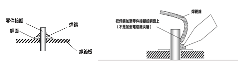
a. Solder Paste Printing
This requires the use of a stencil. The stencil is designed with openings according to the PCB pad layout, and the thickness of the stencil corresponds to the thickness of the solder paste. Since the quality of solder paste printing directly affects the subsequent soldering quality, parameters such as squeegee speed and pressure need to be carefully adjusted before solder paste printing.
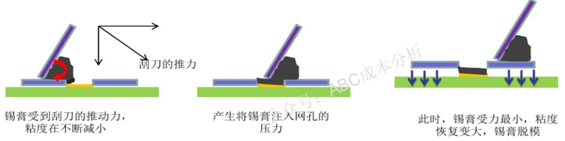 The fixture required for solder paste printing is the stencil, which is specialized and determined by the PCB design, with prices ranging from 300 to 1000 RMB per piece depending on the process. The consumable required for solder paste printing is solder paste, which can be classified into leaded and lead-free types. Due to increasingly stringent environmental requirements, lead-free solder paste is more commonly used, although it is generally more expensive than leaded solder paste. Different types of solder paste should not be mixed, and solder paste needs to be warmed and stirred before use.
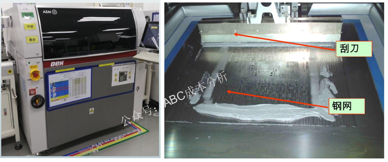 Currently, stencils on the market can be classified into chemical etched stencils, laser cut stencils, electroformed stencils, hybrid stencils, and electropolished laser stencils. Below is a summary of the relevant information for each type of stencil for your reference.

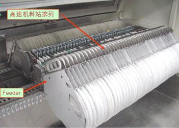
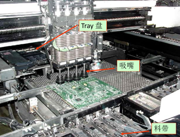
b. Surface Mount Technology (SMT) P&PAlso known as SMT (Surface Mount Technology). SMT requires specialized placement programs; a universal feeding system; and in most cases, the nozzles are universal, although some irregular components may require manufacturers to develop specialized systems.
SMT machines can be categorized by function:
-
High-speed machines: Primarily for components like resistors and capacitors with regular shapes.
Typically contain 10-15 working heads, each capable of swapping 2-5 nozzles.
Placement speed: 10+ components/second.
Each SMT line usually has 1-3 high-speed machines.
High-speed machines may have material throwing issues, so the material preparation during the sample phase should not be based on the actual board quantity; it is best to reserve a 10% buffer.
-
Universal machines: Capable of placing large and irregular components.
Typically contain 3-5 working heads, each capable of swapping 2-5 nozzles.
Placement speed: 1-2 seconds/component for tape, 1-3 seconds/component for trays.
Each SMT production line usually has 1 universal machine.
SMT machines can also be categorized by placement speed:
-
Medium-low speed machines have a theoretical placement speed of below 30,000 pieces/hour (for chip components).
-
High-speed machines have a theoretical placement speed of 30,000-60,000 pieces/hour.
-
Ultra-high-speed machines have a theoretical placement speed exceeding 60,000 pieces/hour.
c. Component Soldering– Reflow Soldering
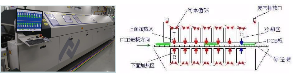
This process melts the solder and forms a reliable connection between the component pins and the PCB pads. Reflow soldering is a specific operation in the SMT process, where inert gas is circulated in the reflow oven to ensure a high-temperature gas atmosphere, re-melting the solder paste distributed on the pads, which solidifies after cooling. Reflow soldering typically uses nitrogen, although there are also vacuum reflow soldering devices.Since reflow soldering can only perform single-sided soldering, if it is a double-sided SMT, the second side must undergo reflow soldering after the first side is completed. Since the temperature at which solder paste solidifies is higher than the reflow soldering temperature, components on the reverse side will not fall off.
 After reflow soldering is the most common point for detecting defects in PCBA, but the causes of defects may not necessarily be due to issues during the reflow soldering process; they could also stem from solder paste printing or placement issues, or related to the solderability of the PCB and component surfaces. However, these problematic areas will only be discovered after reflow soldering. Below is a process of defect formation; in this small animation, during the melting of the solder paste, uneven tension on both sides of the component causes it to stand up, resulting in an open circuit. This situation may arise from poor solder paste printing or improper placement.
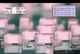 The most critical aspect of reflow soldering is the temperature curve. For example, during the preheating phase, the flux begins to evaporate; if the temperature curve is too steep at this point, and insufficient time is allowed for the venting process before moving on to the soldering and cooling steps, voids in the solder can form, leading to defects. Below is a schematic of the reflow soldering temperature curve.
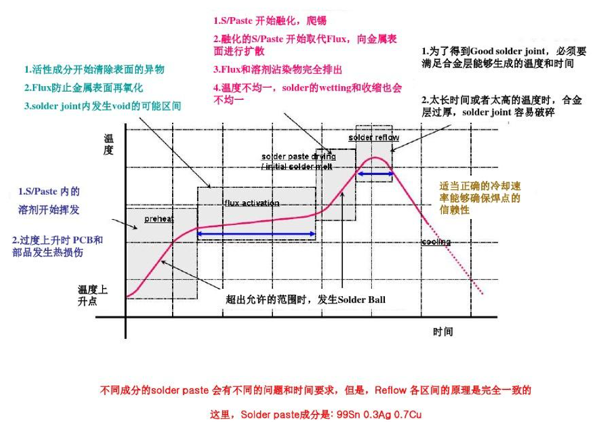 Generally, the solder paste data sheet will provide recommended temperature curves. When adjusting the temperature curve, the following are needed: temperature sensors/wires; calibrated thermometers; PCB boards or actual assembly boards. The temperature curve settings require SMT engineers to repeatedly test based on the solder paste manual, combined with the temperature measuring device and actual assembly board; the more adjustable temperature zones, the better the temperature curve.
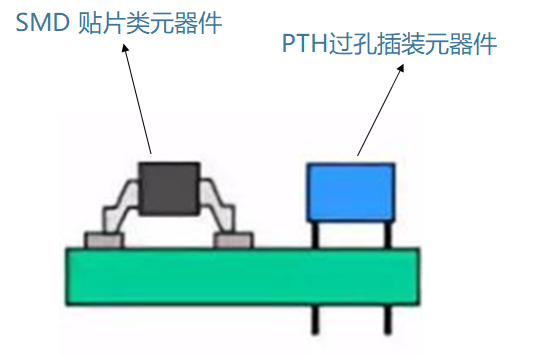
c. Component Soldering–Through-hole components
SMT is only suitable for soldering surface mount devices (SMD); through-hole components (PTH) require other soldering processes:
c1. Wave Soldering
-
Utilizes high temperature to melt solder (solder bar) into liquid solder.
-
Forms a specific shape of solder wave at the surface of the solder pot.
-
Places the PCB with inserted components on a conveyor belt at a certain angle and immersion depth to achieve solder joint soldering.
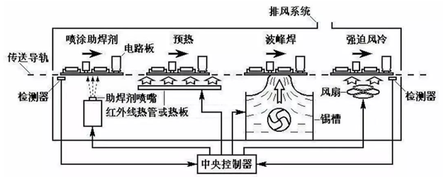
Reflow soldering heats from above, while wave soldering uses the solder wave from below. The disadvantages of wave soldering include:
-
There cannot be components near the solder joint area, as the range of the solder wave is large, and if there are components nearby, they may fall off.
-
Components on the soldering surface are easily affected by thermal shock.
-
The PCB experiences significant thermal shock, making it prone to warping and deformation.
-
There is a lot of melted liquid solder in the solder pot, and if the line stops, there will be significant waste of solder material.
Wave soldering has two forms: single wave and double wave.
-
For single wave, there is only one wave, which is a laminar wave.
-
For double wave, the first wave is called the disturbed wave, and the second wave is called the laminar wave.
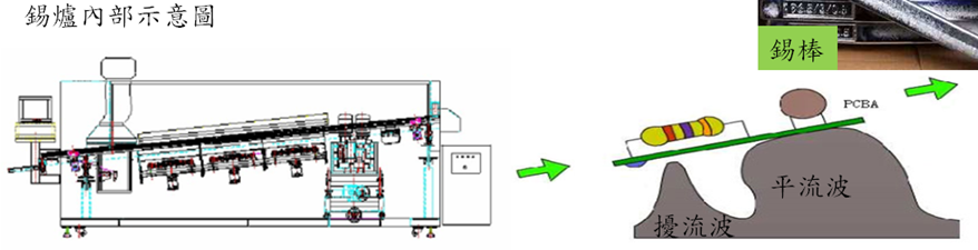
Disturbed wave
-
The disturbed wave can basically complete the soldering.
-
The solder in the disturbed wave moves actively, passing through narrow gaps at high speed, ensuring uniform solder distribution.
-
However, it can easily leave uneven and excess solder on the solder joints, which is why a second wave, the laminar wave, is needed.
Laminar wave
-
The entire wave surface remains basically horizontal, like a mirror surface. At first glance, it seems that the solder wave is static, but in reality, the solder is continuously flowing, just that the wave peak is very stable.
-
Function: Helps eliminate solder spikes and short circuits caused by the disturbed wave.
c2. Selective Wave Soldering (SWS)
SWS stands for Selective Wave Soldering. The soldering process is similar to wave soldering: board entry → flux spraying → preheating → soldering → cooling → board exit, with the differences being:
- Components on the soldering surface are not affected
-
Less thermal shock
-
Less solder waste
-
Stable soldering quality, easier to control.
The disadvantages of wave soldering: when there are many solder joints, the soldering efficiency is not as high as traditional wave soldering.
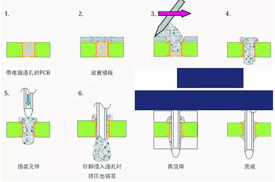
c3. Through-hole Reflow Soldering (THR)THR stands for Through-hole Reflow. In simple terms, it allows through-hole components to be soldered together with SMD components during solder paste printing, placement, and reflow soldering processes.
-
Advantages: Since the entire process is completed with SMT, it can save one subsequent soldering process.
-
Disadvantages: Ordinary PTH components have low temperature resistance requirements, but THR components need to withstand higher temperatures (the maximum temperature for reflow soldering is about 250-260 °C), thus increasing material costs.
c4. Automatic Spot WeldingAutomatic spot welding simulates the manual spot welding process using automated machinery, utilizing robotic arms and temperature control for welding, requiring programming to edit the welding path, temperature, and time.
d. Board Separation Routing/Punch/V-Cut To improve production efficiency, PCBA is produced in panel form until the board separation step. After separation, PCBA is produced in single-piece form.Separation methods include:
d1. Manual Breaking
Typically used in the initial sample stage to save on fixture costs, manual breaking requires the PCB to be processed into postage stamp holes to facilitate manual separation.
d2. Punching Board Separation Machine (Punch)
-
The die cuts directly above the PCB, separating it.
-
Advantages: Low equipment cost, fast speed, high efficiency.
-
Disadvantages: Requires dedicated dies for each board, which can be costly.
-
Using a punching method on rigid boards can create significant stress, potentially damaging components.
-
More suitable for flexible boards, which do not have stress issues.
d3. Router-type/Board-type Separation Machine (V-Cut)
-
Advantages: Low cost, low equipment price, and generally no need for fixtures.
-
Disadvantages: Can only perform straight cuts, may leave burrs, and requires V-grooves to be opened on the PCB.
d4. Milling-type Separation Machine (Routing)
-
The most common separation method for rigid PCBs, using milling processing.
-
Advantages: Can perform cuts of any shape, with minimal stress and no burrs on the cutting edge.
-
Disadvantages: High equipment costs. Fixtures are used for positioning and covering components, which are not expensive, but milling cutters are consumables that wear out quickly.
d5. Laser Separation Machine (Laser)
-
Advantages: Retains the benefits of milling-type separation machines and can perform micro-cutting on PCBs without stress.
-
Disadvantages: Equipment is expensive.
e. Programming OBP OBP stands for On Board Programming. If IC components are mounted on the PCBA, it may be necessary to program the software into the IC, with the programming software generally provided by the customer.02
ABC Sharing Session
Logistics Operations
Board Loading/Unloading/Circulation/Buffering
Traditional board loading method: Manual loading, with one operator responsible for labeling and loading.
Automated board loading method: Automatic coding and loading.
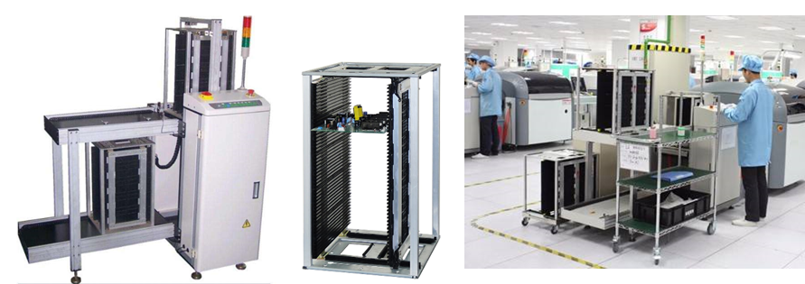
Considering efficiency and the rising labor costs, more and more companies are adopting automated methods for board loading, leading to the development of a complete PCB loading/unloading/circulation/buffering system, which includes multiple devices. Below is a system configuration we found online for your reference.
-
Multi Magazine Loader: Multi-layer board loader
-
Turn Conveyor: Turning board loader
-
Destacker: Board suction machine
-
High Speed Laser Masking: High-speed laser coding machine
-
Work Station: Work station
-
FIFO Buffer: First In First Out temporary storage machine
-
Dual Unloader: Dual unloading machine
03
ABC Sharing Session
Quality Control Operations
a. Incoming Quality Control (IQC)
When parts arrive, they need to undergo full inspection or sampling inspection before being accepted into inventory. The entire inventory process is traceable, and information such as the inventory date, material inspection report, and even the supplier’s production batch can be traced through the barcode or QR code on the part packaging.
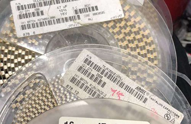
Different parts require different inspection contents, and the corresponding inspection equipment also varies. Below are some common inspection contents for materials:
-
PCB: Sampling dimensions, 100% full inspection of dimensions for the first batch of incoming materials.
-
Electronic components (resistors/capacitors/diodes/chips, etc.): Sampling resistance/capacitance values, etc.
-
Connectors: Sampling impedance.
-
Wiring harnesses: Sampling impedance.
-
Structural parts: Sampling dimensions, 100% full inspection of dimensions for the first batch of incoming materials.
Tips : How to Understand Incoming Material Information?The label on the part contains a lot of information, which may seem overwhelming at first glance, but with patience and careful verification, we can obtain a lot of information. For example, from the label below, what can we learn?
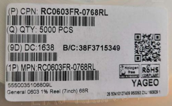
CPN: Customer Part Number, which is the customer model or part number.QTY: Quantity, which is the incoming quantity. Generally, resistors and capacitors come in specifications of 3000 pieces/roll and 5000 pieces/roll.
DC: Date Code, which indicates that this part was produced in the 38th week of 2016.
B/C: Batch Code, which is used for internal traceability by component manufacturers. When quality issues arise, manufacturers often request the B/C for internal inquiries.
MPN: Manufacturer Part Number, the original manufacturer’s model or part number.
QR Code: Contains relevant traceability information from the manufacturer.
ROHS: This is an environmental mark. ROHS is a mandatory standard established by EU legislation, officially known as the “Directive on the Restriction of the Use of Certain Hazardous Substances in Electrical and Electronic Equipment”.
YAGEO: Name of the original manufacturer (not the agent).
Tips: How to Understand MPN?
- Visit the component manufacturer’s official website to obtain the component datasheet and check the MPN naming rules.
- Search for “MPN” or “PN” to quickly find the section explaining the coding rules.
For example, in the case of RC0603FR–0768RL:
- RC: Series number.
- 0603: Size code, where 0603 indicates 0.6 inches * 0.3 inches, and so on.
- F: Resistance tolerance, defined by YAGEO as:B=+/-0.1%D=+/-0.5%F=+/-1.0%J=+/-5%
- R: Packaging type.
- -: Temperature coefficient of resistance, where “-” indicates based on detailed specifications.
- 07: Reel diameter, where 07 indicates a reel diameter of 7 inches.
- 68R: Resistance value, where 68R indicates a resistance of 68Ω.
- L: System default code.
b. Label Tracking
This includes tracking during production and subsequent tracking. During production, each station scans the label on the PCB to intercept defective products in a timely manner, preventing defective products from reaching the client.
Common label forms include:
-
Traditional paper labels (anti-static, high-temperature labels): Methods include label printing and manual/automated label application.
-
Inkjet printing
-
Laser engraving
The content of labels/printing/engraving includes: text or barcodes/QR codes.
The content of text/barcodes/QR codes varies by company, but generally includes part numbers, batch numbers, date codes, etc.
c. Solder Paste Inspection (SPI) This station aims to inspect the quality of solder paste printing, primarily measuring the height of the solder paste, which can be divided into online and offline forms. Offline inspection typically involves full inspection of the first 10-20 pieces, followed by continuous inspection of the first piece for every 5 pieces and sampling every 2 hours; while online solder paste inspection usually involves 100% online checks to prevent defective solder paste from entering the next station. Different companies may have varying inspection requirements, so it cannot be generalized.
The working principles of solder paste inspection are based on two methods: laser scanning optical inspection and moiré fringe optical inspection.
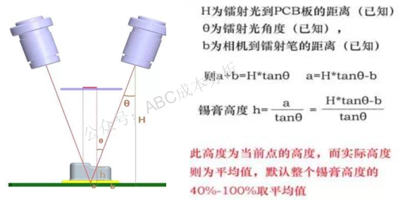
c1. Laser Scanning Optical Inspection
-
Measures solder paste height.
-
Calculates the current height of the solder paste at each point using laser and trigonometric principles.
-
Obtains height values for each monitoring point through calculations.
-
Simulates the shape/surface distribution of the solder paste using the height values of each monitoring point.
-
Feedbacks abnormal points where the height does not meet standards.
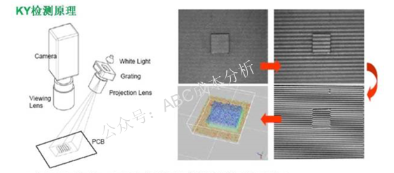
c2. Moiré Fringe Optical Inspection:
-
A white light source projects a pre-defined, periodically varying, stripe pattern onto the solder paste through a grating.
-
A high-resolution CCD camera (1-4M pixels) captures four images within one cycle (four quadrants), each containing height information for every pixel.
-
By comparing the four images, the height values for each pixel are obtained.
-
Simulates the shape, surface distribution, and volume of the solder paste using the height values for each pixel.
-
Feedbacks abnormal points where the height does not meet standards.
 d. Automatic Optical Inspection (AOI)Inspects for solder defects after reflow soldering. It is important to note that AOI can only check components with solder joints visible from the top; if the solder joints are not visible from the top, automatic X-ray inspection equipment is needed to check for solder defects.
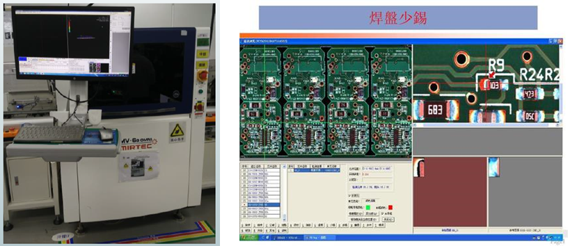
d1. AOI Inspection Principle:
-
The camera automatically scans the PCB to collect images.
-
In the initial phase, a Golden Sample is used to establish a qualified image database.
-
The system automatically compares the solder joints with the qualified images in the database to identify defects on the PCB.
-
Defects are highlighted on the display for repair personnel to address.
d2. AOI Inspection Working Logic:
-
Image acquisition phase (optical scanning and data collection).
-
Data processing phase (data classification and conversion).
-
Image analysis phase (feature extraction and template comparison).
-
Defect reporting phase (classification of defect size and type, etc.).
d3. AOI Equipment Hardware System:
-
Working platform.
-
Imaging system.
-
Image processing system.
-
Electrical system.
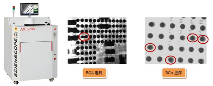
e. Automatic X-ray Inspection (AXI)
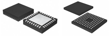
Can inspect solder joints on components that are not visible from the bottom, such as components using BGA ball grid array packaging. AXI equipment can be either online or offline.
The detection principle is similar to a CT scan in a hospital:
-
There is an X-ray emitter above the PCB.
-
The X-ray passes through the PCB and is received by a detector placed below the PCB.
-
Solder joints contain a large amount of material that absorbs X-rays, appearing as black spots in the image.
-
Materials like fiberglass/copper absorb less X-rays, appearing as gray areas in the image.
-
By adjusting the black/gray contrast, solder defects (bridging, cold solder, bubbles, etc.) at the bottom of components can be visually identified.
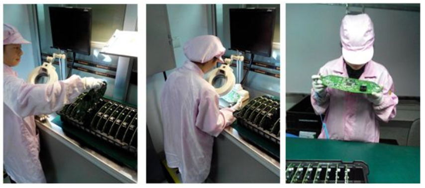
f. Manual Visual InspectionManual visual inspection is a supplementary check to AOI and AXI. The inspection standard document is IPC-A-610-F; generally, the required tools include magnifying glasses, low-power microscopes, computers, and barcode scanners.
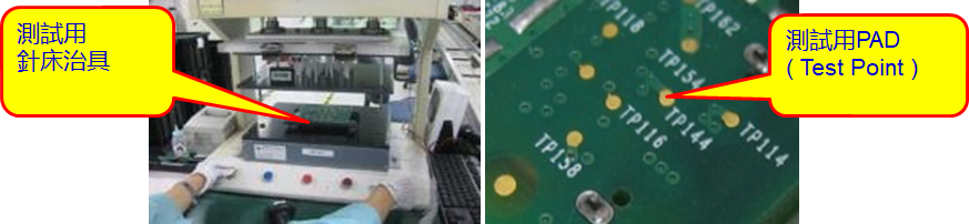
g. In-Circuit Testing (ICT)
ICT stands for in-circuit testing. ICT can be performed before or after board separation; testing before separation is more efficient but cannot detect defects caused by separation (component damage/solder cracks/open circuits, etc.).The testing principle of ICT can be imagined as a high-end multimeter, except that a multimeter can only test one component at a time, while ICT can test multiple components on the PCBA simultaneously.
- The bed of nails presses down, contacting the pre-reserved test points on the PCB, similar to using a multimeter to measure resistance by touching the probes to both ends of the resistor.
- One can think of a string or part of a circuit as a component and measure its equivalent resistance/capacitance/voltage (reducing the number of test points).
- ICT has coverage issues; due to the limited number of test points, it may not achieve 100% coverage. Excellent test point design can improve test coverage.
h. Function Testing (FCT)FCT stands for Function test, which aims to check whether the entire PCBA meets design objectives and operates normally. FCT equipment varies greatly in price depending on testing requirements, testing time, and the original intent of the equipment.
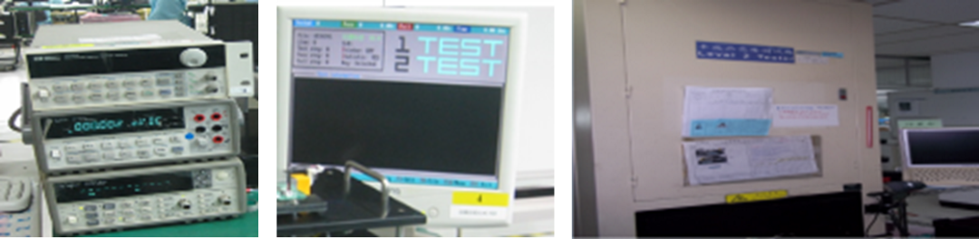
- Treats the PCBA as a functional entity, providing input signals and checking output signals according to the design requirements of the functional entity.
-
Testing requirements and equipment vary based on the original intent, leading to significant price differences.
Process Costs Product Costs Cost Management & Cost Reduction Cost Vocabulary