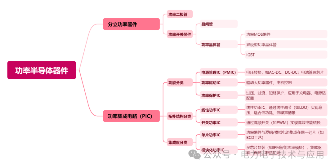
Power semiconductors are the core of energy conversion and circuit control in electronic devices, primarily used for changing voltage and frequency, as well as DC to AC conversion. Power semiconductors can be divided into two main categories: Power ICs (Power Integrated Circuits) and Power Discrete Devices (including power modules). Power devices refer to the discrete components of power semiconductors, while Power ICs integrate power discrete devices with peripheral circuits for driving, control, protection, interface, and monitoring. MOSFET, short for Metal-Oxide-Semiconductor Field-Effect Transistor, belongs to the category of power discrete devices and is an important classification within Field Effect Transistors (FETs). It is a voltage-controlled semiconductor device characterized by high operating frequency, low power consumption, high input impedance, low on-resistance, high energy efficiency, large dynamic range, ease of integration, absence of secondary breakdown phenomena, and a wide safe operating area. It has become a strong competitor to bipolar transistors and power transistors.
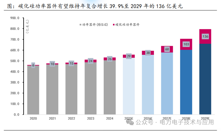
 Global Power Semiconductor Market: Third-Generation Semiconductor Materials Maintain High Growth• The market size for power discrete devices and power modules in 2023 is $35.7 billion, shrinking to $32.3 billion in 2024, with a compound annual growth rate (CAGR) of 7.14% over the past decade.• In a broad sense, the global power device market (including SiC) is projected to reach $53.06 billion in 2024, with a CAGR of 3.55% from 2020 to 2024. As third-generation semiconductor materials accelerate their penetration, the global power device market is expected to maintain an 8.43% CAGR, reaching $79.53 billion between 2024 and 2029.• Third-generation semiconductor materials continue to grow rapidly: new wide bandgap material power semiconductors are experiencing high growth rates, with a CAGR of 45.4% for silicon carbide (SiC) power devices from 2020 to 2024. According to Omdia and Yole forecasts, the global SiC power device market is expected to maintain a CAGR of 39.9%, reaching $13.6 billion between 2024 and 2029.
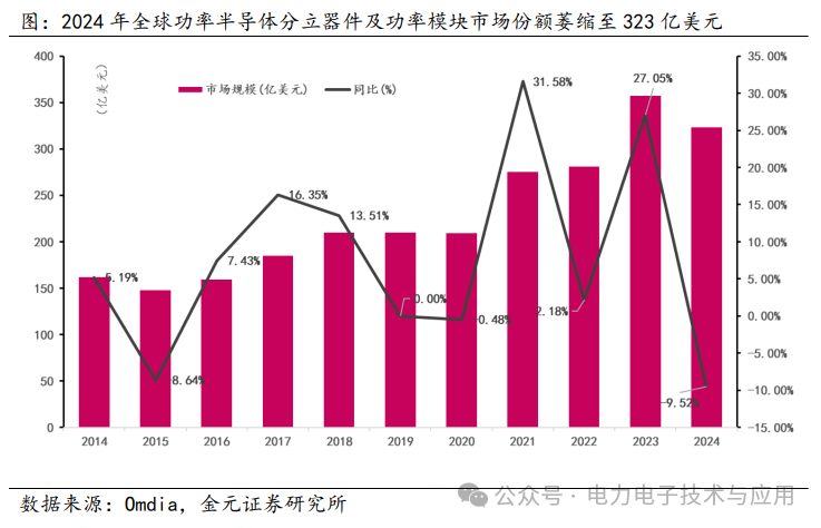
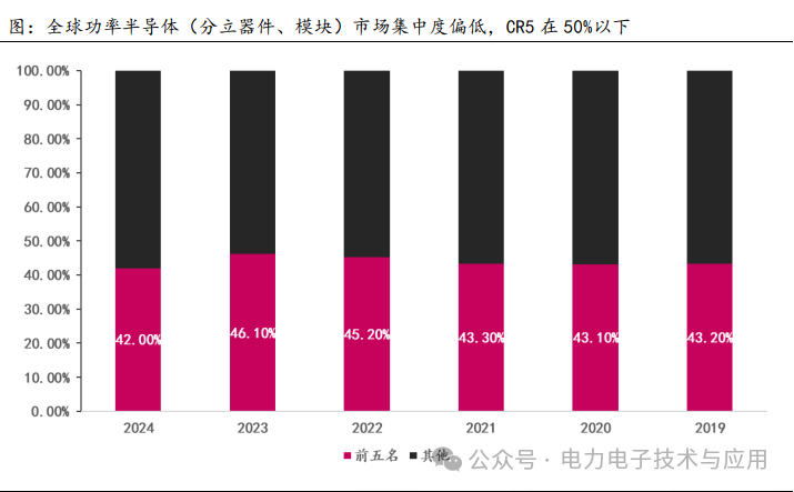
 Global power semiconductors (discrete devices and modules) are relatively fragmented, but leading companies are primarily foreign enterprises.• In 2024, Infineon holds the largest market share in global power semiconductors (discrete devices and modules) at 20.8%; the second is ON Semiconductor with a market share of 9.2%; Chinese company Silan Micro holds a market share of 3.3%, an increase of 0.7 percentage points from 2023. BYD’s market share continues to rise, ranking seventh globally.• Compared to automotive-grade power semiconductors, the concentration of power discrete devices and modules is relatively low and fragmented, with a CR5 below 50%. However, foreign enterprises dominate, with Infineon maintaining a stable market share of around 20%, indicating significant domestic replacement potential.
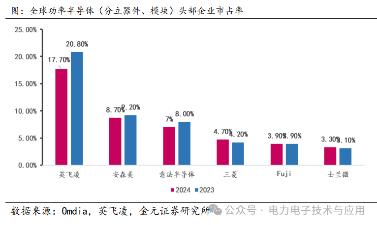
 China is the largest consumer of power semiconductors globally.• As the largest consumer of power semiconductors globally, China contributes approximately 40% of the power semiconductor market. According to forecasts from Omdia and the China Business Industry Research Institute, the domestic power semiconductor market size is expected to be approximately 151.936 billion yuan in 2023, growing to 175.255 billion yuan in 2024.• In terms of market structure, power integrated circuits, including power management chips, driver chips, AC/DC converters, etc., account for the largest share; discrete devices such as MOSFETs, power diodes, and IGBTs account for 16.4%, 14.8%, and 12.4%, respectively.
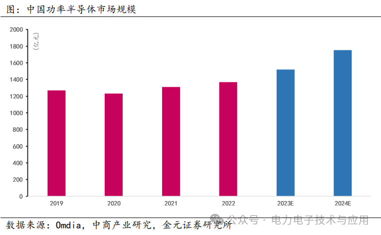
 Power semiconductors are evolving from “single devices” to “system-level solutions”.• Power processing includes: frequency conversion, voltage transformation, current conversion, power amplification, power management, etc. Currently, the 4C market, represented by automotive electronics, computers, communications, and consumer products, occupies the majority of the power semiconductor application market. Improvements in high-voltage lateral power device structures have also led to the emergence of the monolithic power integrated circuit market.• Power semiconductor devices used in applications in the computer, communication, and automotive industries have voltage ratings below 200V; power semiconductor devices used in applications for electric control, robotics, and power distribution have voltage ratings exceeding 200V. The application of power devices is a function of operating frequency. High-power systems (such as high-voltage direct current transmission and locomotive drive systems) perform megawatt-level power control at relatively low frequencies. As the operating frequency increases, the rated power for typical microwave devices at 100W decreases.
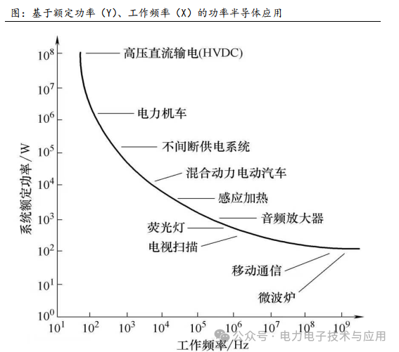
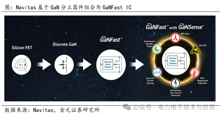
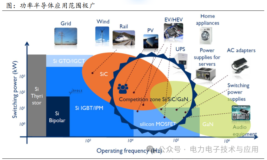 • Power semiconductors are evolving from “single devices” to “system-level solutions”, becoming the “heart” of smart terminals, energy networks, and industrial systems.• Through packaging and integration technologies such as 3D Packaging, Embedded Die, and SoC, power modules can be packaged or integrated into a single chip, reducing interconnection losses and improving power density. For example, Infineon uses Embedded Power technology to directly embed MOSFETs into PCB substrates, reducing inductance and thermal resistance, gradually optimizing its revenue structure. By integrating product portfolios, Infineon’s ATV division achieved a 24% CAGR from FY2020 to FY2024, with power devices still accounting for a significant proportion.• Similarly, Navitas provides GaNFast, which combines multiple power discrete devices into a single GaN IC to enhance speed, efficiency, reliability, and cost-effectiveness.
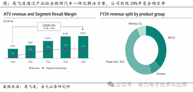
 New energy vehicles open up growth space for IGBTs and SiCs, while the market share of domestic automotive-grade semiconductors needs to be improved.
• According to the S&P Automotive Semiconductor Tracker, the pure electric BEV market is expected to reach 11 million units in 2024, with an estimated growth to 32 million units by 2030, representing a CAGR of about 20%.
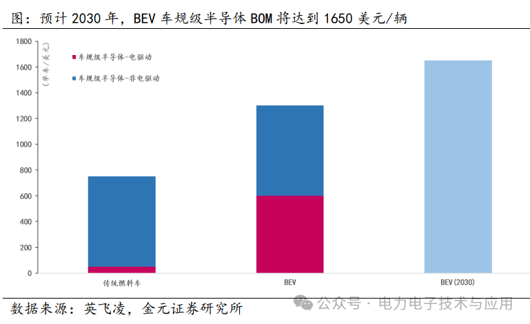
• Benefiting from high voltage and high power requirements, material iterations, and SDV (soft design vehicle) drives, Infineon predicts that the semiconductor BOM (Bill of Materials) for BEVs will increase from $1,300 per vehicle in 2024 to $1,650 by 2030 (up to $2,500 for high-end models). In addition to the high power demand from the drive system, ADAS, comfort, and safety features also drive the BOM for semiconductors per vehicle.
• IGBT power modules play a core role in motor controllers, directly controlling the conversion of DC and AC power, while also performing frequency control on AC motors. They directly influence the acceleration capability and maximum speed of new energy vehicles by determining the torque and maximum output power of the drive system, making them the core of the core.
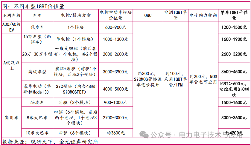
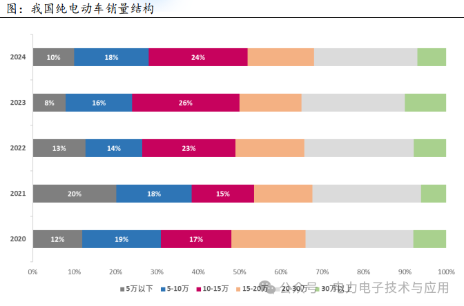
• The cost of IGBT in new energy vehicles is closely tied to vehicle positioning and system power requirements, with significant structural differences in market value distribution. From a functional module perspective, the value of the main drive electric control system IGBT is approximately 1,000 yuan, responsible for core energy conversion functions, while the value of IGBTs in subsystems such as OBC, air conditioning compressors, and electronic power steering is below 300 yuan, collectively accounting for about 25%-30%. In terms of vehicle classification, higher-end models are equipped with more power modules, resulting in higher value. The IGBT value for A00/A0 level new energy vehicles is between 600-900 yuan, while for high-end models, it ranges from 3,000 to 3,900 yuan. In terms of sales structure, the proportion of mid-to-low-end models (below 200,000 yuan) is gradually increasing. From the structure of pure electric vehicles in China, the proportion of models below 200,000 yuan has increased from 66% in 2020 to 68% in 2024, with the incremental growth mainly coming from models priced between 100,000 and 150,000 yuan. Relatively speaking, the cost of IGBTs is lower, and the likelihood of mid-to-low-end models using SiC is low.
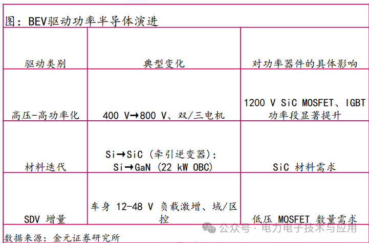
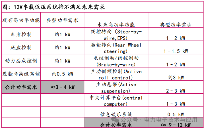
• The traditional 12V vehicle low-voltage system can no longer support the next generation of vehicles (especially for autonomous driving and regional E/E architecture) due to the surge in power demand, necessitating an upgrade to a 48V low-voltage platform. High-power functions continue to be added as the level of autonomous driving increases, requiring numerous electromechanical actuators such as electric power steering, electronic braking, electronic steering, active suspension, and active roll stabilization, all of which belong to kW-level loads.
• PowerP = 𝑈𝐼. At a fixed target power, if the voltage is only 12V, the current becomes excessively high → the cross-sectional area of the wiring harness, weight, copper loss, and heat generation all increase exponentially, making it neither economical nor safe. The 48V system balances efficiency and safety advantages. Compared to 12V, it can reduce the current to 1/4, significantly lowering the weight of the wiring harness and thermal losses, while still remaining within the safe low-voltage range (<60V DC). The regional E/E architecture + autonomous driving requires nearby power supply in various areas of the vehicle, and the 48V bus naturally matches with the Zone Controller, shortening wiring and enhancing redundancy.
• The market size for 48V MOSFETs, SiC high-voltage DC/DC converters, and intelligent driver ICs will expand in tandem with electric vehicles and L3+ autonomous driving.
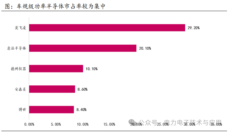
 • The proportion of new energy vehicle shipments in China continues to rise, exceeding 50%: the domestic shipment of new energy vehicles has remained stable at over 50% since 2022, with the monthly shipment approaching 60% in 2024, and continuing to rise.• There is a significant disparity between the market share and sales of domestic automotive-grade power semiconductors: benefiting from the global penetration rate of new energy vehicles and the increased usage of power semiconductors and power ICs in new energy vehicle power systems compared to traditional fuel vehicles, the global automotive-grade semiconductor market size has grown from $37.2 billion in 2019 to $68.38 billion in 2024. However, the current concentration of automotive-grade power semiconductors is much higher than that of power discrete devices and modules. The top three are Infineon, STMicroelectronics, and Texas Instruments, with market shares of 29.20%, 20.10%, and 10.10%, respectively.
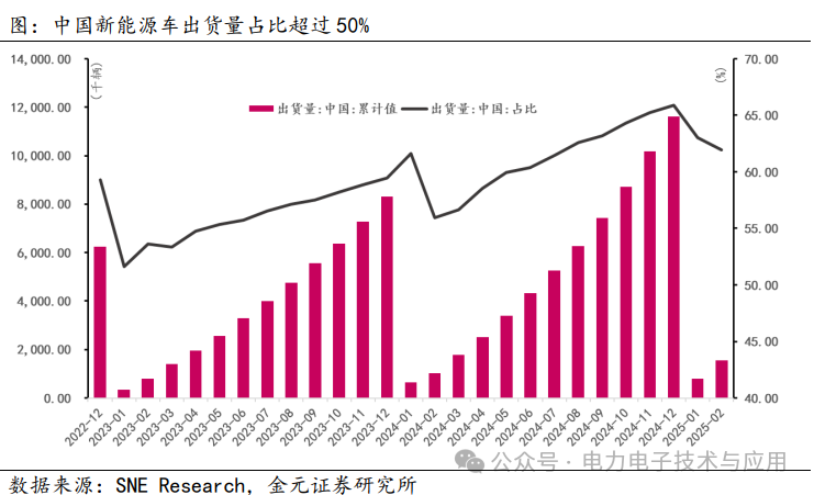
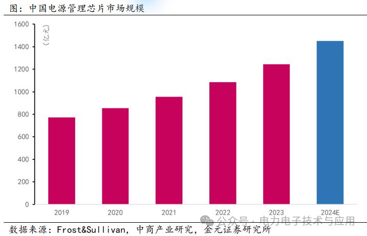
 3C Field Catalyzes Demand for Power Management Chips• Consumer electronics, such as smartphones and tablets, catalyze the demand for power management chips. A flagship smartphone typically requires 10-15 PMIC/power sub-chips internally, with each integrating 2-4 pairs of power MOSFETs, resulting in over 20 pairs of low-voltage MOSFETs in a single phone. As smartphones become increasingly advanced, the demand for complex PMICs has surged to support features such as 5G connectivity, AI processing, and high-resolution displays. These components are crucial for managing battery life, thermal performance, and overall device efficiency, directly impacting user experience and device lifespan.• In 2023, the market size for power management chips in China reached approximately 124.3 billion yuan, with a compound annual growth rate of 12.60% over the past five years. The market size for power management chips is expected to be around 145.2 billion yuan in 2024.
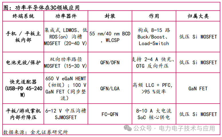
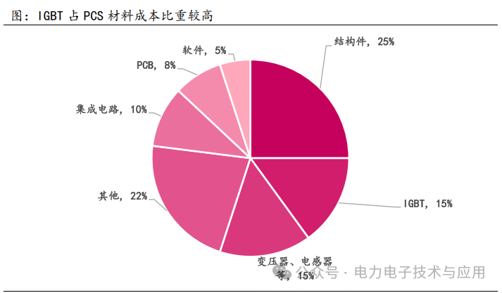
 Energy Storage and AI Computing Center Construction May Become a New Growth Curve for Power Semiconductors• Energy storage converters (PCS), also known as bidirectional energy storage inverters, are the core components that enable bidirectional energy flow between energy storage systems and the grid, controlling the charging and discharging processes of batteries and performing AC/DC conversion. In battery energy storage systems, they account for about 15%-20% of the total cost and are a key core component. PCS is responsible for bidirectional energy exchange between the AC grid (380V/480V three-phase) and the DC battery string (650V-1,500V). The ability to minimize charging and discharging losses and to make the cabinet smaller and cooler largely depends on the selection of power devices.• In energy storage converters, material costs account for about 93%, with the highest proportion being structural components (about 25%), followed by IGBTs (about 15%) and magnetic components such as transformers and inductors (15%).• SiC has great potential in the energy storage field: PCS target efficiency ≥ 98%, and SiC’s on-resistance and reverse recovery losses are far lower than those of traditional IGBTs, which can reduce losses by 30-50%, alleviating the burden on air conditioning or liquid cooling. KACO’s blueplanet gridsave 92.0 TL3-S is the first battery inverter to use SiC power modules, showcasing an outstanding efficiency of up to 98.8%.
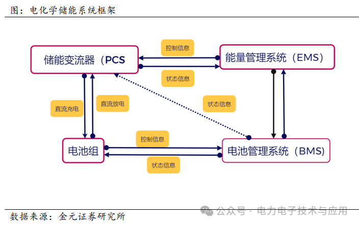
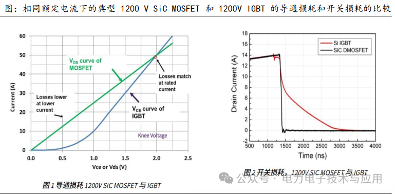
 • Global energy consumption of computing devices is expected to surge significantly with the explosion of AI demand. Computing devices are a major source of energy consumption and carbon emissions. From 2024 to 2030, AI chips will bring an annual new demand of 4 to 9 GW for data center IT equipment loads, accounting for about 70% of the new IT equipment load in data centers.• Reducing transmission losses is a key focus for power supply and distribution systems. Traditional power supply and distribution systems are complex, including transformers, UPS, distribution cabinets, and multiple sets of equipment, while traditional UPS power supply solutions have significant energy losses and low efficiency. Energy-saving technologies such as efficient UPS, smart online UPS modes, and power modules have begun to be applied on a large scale.• Achieving high efficiency relies on the application of third-generation semiconductor materials. Wide bandgap semiconductor devices such as silicon carbide (SiC) and gallium nitride (GaN) are gradually penetrating the PSU (Power Supply Unit) field. Research by Wolfspeed indicates that under low load conditions, the conduction losses of 1200V SiC MOSFETs are only half that of 1200V IGBTs at the same drive current, and by eliminating the turn-off tail current, their switching losses can be reduced by up to 90% compared to IGBTs.
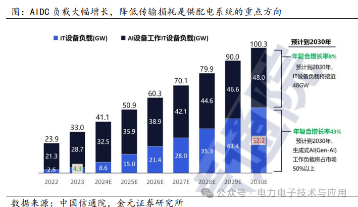
 • Mainstream AI training cabinets are being upgraded from traditional 10-15 kW to over 30 kW, with high-end liquid-cooled cabinets even reaching 100 kW. A high-density AI server cabinet can have power semiconductor materials costing as much as $12,000 to $15,000, including 24 PSUs, 36 GPU boards, 18 48V bus conversion boards, and over 300 protection devices.
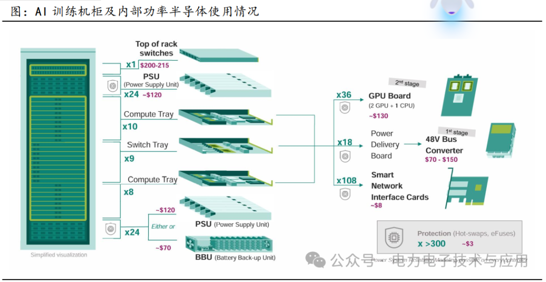 AI drives megawatt-level power demand, and 800V HVDC relies on high-performance power semiconductor materials.
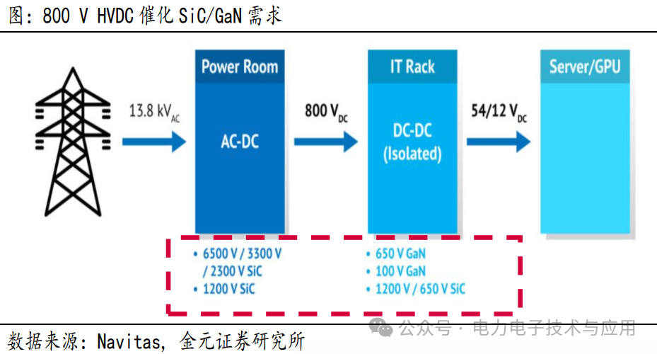
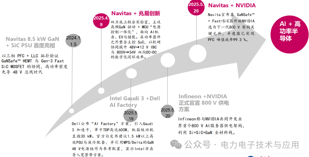 AI drives megawatt-level power demand, and 800V HVDC relies on high-performance power semiconductor materials.• In the era of AI-driven data centers, kilowatt-level power standards can no longer meet the extreme energy demands of AI models. Taking the GB200 NVL72 rack as an example, as the rack power approaches megawatt levels, the traditional distribution method based on 54V DC has reached a bottleneck. The excessive current in a 54V system requires large copper busbars and power racks. In megawatt-level Kyber computing nodes, the power supply alone can consume the entire rack space, leaving no room for computing resources. NVIDIA estimates that a megawatt-level rack using a 54V DC architecture could require power equipment as high as 64U rack units, making it impractical for real-world deployment. The 54V distribution chain typically includes multiple stages of AC/DC and DC/DC conversion, with each energy conversion representing a risk point, significantly impacting the overall efficiency and increasing potential failure points and maintenance costs.• The 13.8kV AC power entering the data center is converted to 800V HVDC at the boundary through industrial-grade rectifiers, and then transmitted directly to the equipment racks and IT racks via two wires, achieving a highly simplified power flow path of “one-time AC conversion, full DC transmission.” The new 800V high-voltage direct current (HVDC) centralized power supply method relies on the support of high-performance power semiconductor materials.
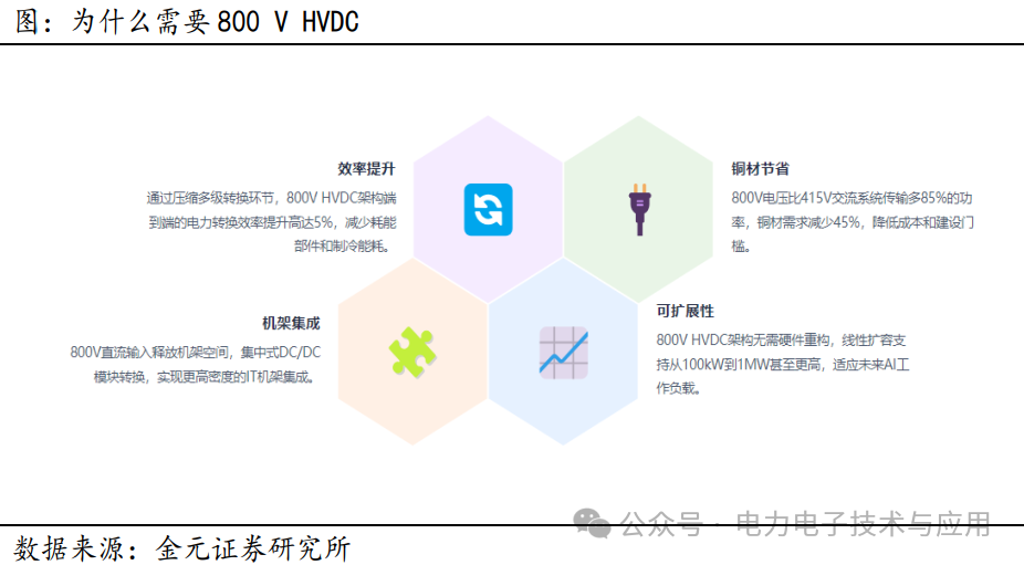
 Power Semiconductors Based on Material Classification• The performance of power semiconductors largely depends on their manufacturing materials. Different materials have different bandgap widths, electron mobility, thermal conductivity, and other characteristics, which determine key parameters such as voltage, current, switching speed, and operating temperature of the devices.
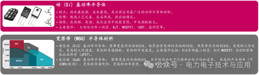
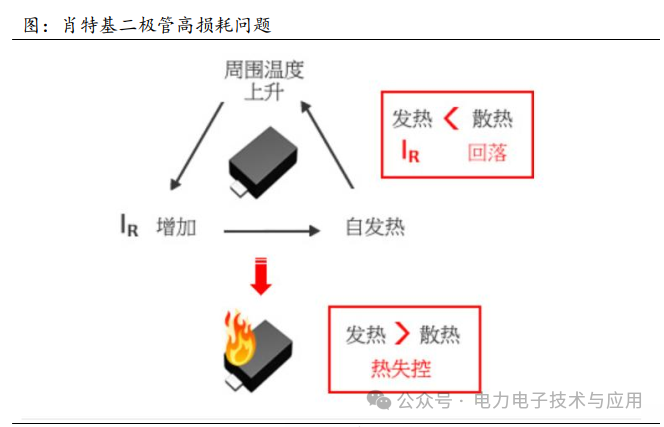
 Traditional Power Diodes Face the Dilemma of “High Voltage vs. Low Loss”• Power diodes are the most basic power devices, allowing current to flow in only one direction, widely used for rectification, commutation, and preventing backflow. Traditional silicon PN junction power diodes form a junction barrier through P-type and N-type semiconductors, and during forward conduction, the injection of minority carriers leads to a forward voltage drop typically above 0.7-1V. Additionally, during the reverse recovery process, the recombination of carriers generates reverse recovery current, resulting in extra switching losses.• Schottky barrier diodes (SBD) replace the PN junction with a metal-semiconductor contact, achieving a rectification mechanism based on majority carrier conduction. The main advantages of silicon Schottky diodes are lower forward conduction voltage (0.4-0.5V, significantly lower than the voltage drop of silicon PN diodes at the same current) and almost “zero” reverse recovery current, resulting in extremely fast switching speeds.• However, silicon Schottky diodes also have limitations. Their reverse voltage rating is limited by the lower bandgap width and critical field strength of silicon materials: to suppress leakage current at high voltage, it is necessary to reduce the doping concentration of the semiconductor and increase the thickness of the drift region, which leads to a significant increase in on-resistance and forward voltage drop. In other words, if one wants to enhance their voltage capability, it will result in increased losses.
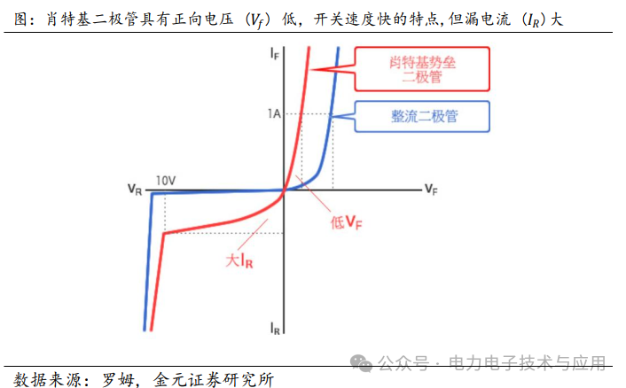
 Super Junction (SJ-MOS) and IGBTs Drive Power MOSFETs into the Era of High Frequency, High Voltage, and Low Loss• Metal-Oxide-Semiconductor Field-Effect Transistors (MOSFETs) are typical unipolar power devices that conduct through minority carriers (majority carriers), thus offering advantages such as fast switching speed and low driving power consumption. Power MOSFETs have been in practical use since the 1980s, achieving operating frequencies in the MHz range, making high-frequency applications such as switch-mode power supplies possible. Silicon power MOSFETs are generally N-channel enhancement types, using gate voltage to induce the formation of an N-channel conduction current in the P-type body region. MOSFETs are voltage-driven devices, with simple gate driving and high input impedance; during conduction, there are no recovery issues like diodes, resulting in low switching losses, making them very suitable for small power converters in high-frequency environments.• In low-voltage (tens to hundreds of volts) applications, silicon MOSFETs can achieve very low on-resistance and low switching losses, thus widely replacing bipolar transistors in communication power supplies, computer VRMs, and household appliance inverters. However, for high-voltage (>500V) applications, the weaknesses of silicon MOSFETs begin to emerge: to withstand high voltage, their N-drift layer must be thick enough and have a low doping concentration, which causes the on-resistance to increase exponentially with voltage rating. The conduction losses of high-voltage MOSFETs are much higher than those of IGBTs and other bipolar devices, making it difficult for MOSFETs to compete in applications above 600V. Additionally, the on-voltage drop of MOSFETs increases linearly with increasing current (Ohmic characteristics), unlike BJTs/IGBTs, which can maintain a low voltage drop even at high currents. Therefore, in kilovolt-level high-voltage high-current scenarios (such as electric vehicle main inverters and industrial drives), traditional silicon MOSFETs are not the best choice.• Traditional MOSFETs are limited by the balance between voltage rating and on-resistance, and the technology has undergone developments such as “double diffusion + vertical conduction” VDMOS, U-shaped trench gate UMOSFET, and trench deepening + bottom extension EXTFET.
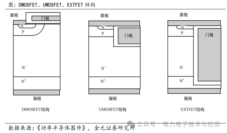 IGBT ≈ BJT + Power MOS, Trench IGBTs May Become the Mainstream Trend
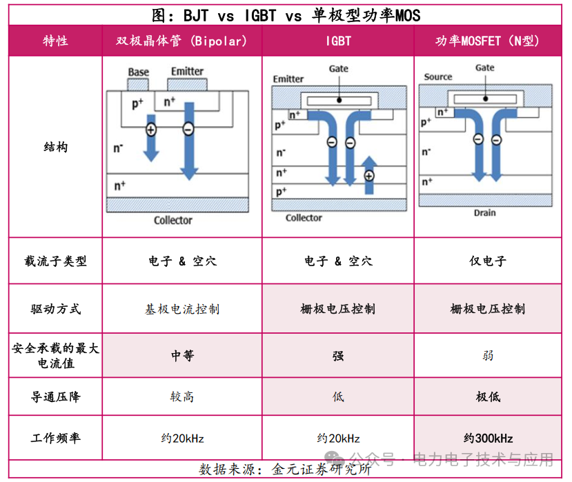 • IGBTs combine the characteristics of MOSFETs and BJTs: the gate voltage triggers the internal MOSFET to conduct, driving holes from the p+ collector into the n- drift region, initiating bipolar conduction modulation, reducing the resistance of the n- region to 1/5-1/10 of that of traditional MOSFETs, achieving low on-voltage drop (1-3V) at high voltages (1200V+). When turned off, the stored carriers in the n- region must dissipate through recombination or extraction, generating tail current and causing turn-off delay (about 100ns). IGBTs exhibit significant performance advantages in medium to low-frequency, high-voltage high-current scenarios (such as electric vehicle inverters) below 20kHz, but their high-frequency characteristics are weaker than those of MOSFETs.• Driving methods: BJTs require continuous base current (high driving power consumption), while MOSFETs/IGBTs only require capacitive charging and discharging (simplifying the driving circuit by over 90%).• Frequency vs. voltage rating trade-off: MOSFETs excel in high frequency and low loss, while IGBTs sacrifice speed for high voltage and high current capability, with BJTs gradually being replaced, remaining only in low-cost linear applications.• Loss mechanisms: BJT/IGBT conduction losses dominate (conduction modulation effect), while MOSFET switching losses are more significant (especially under high frequency).• Trench gate technology is a significant improvement in the structure of power devices, initially applied to low-voltage power MOSFETs and later extended to high-voltage MOSFETs and IGBTs. Compared to traditional planar gate structures, trench devices can achieve higher channel density per unit chip area, thereby reducing on-resistance and increasing current capability.• Trench MOSFETs: Traditional planar MOSFETs (also known as DMOS structures) have their gate located on the chip surface, conducting current through the formation of a horizontal inversion channel on the surface of the P-type body region. There is a certain distance between adjacent P body regions, forming a “JFET effect” area: when the MOSFET conducts, the current must pass through the narrow neck area between the two P regions, generating additional resistance and current crowding effects. Trench MOSFETs (trench gate MOSFETs) vertically etch trenches in the silicon wafer and grow gate oxide on the trench sidewalls, filling with polysilicon as the gate. This changes the contact of the gate with the P body region from planar to vertical sidewall, allowing the channel current to flow vertically along the trench sidewall to the substrate.• Trench IGBTs: The gate of planar gate IGBTs is similar to that of MOSFETs, also located on the chip surface to control the formation of a channel on the surface of the P-well. However, due to the bipolar diffusion current in IGBTs, the JFET effect and uneven carrier distribution issues are more pronounced in their planar structure. Trench IGBTs drive the MOSFET unit of the IGBT by placing the gate in a vertical trench, forming a vertical channel. This allows for a more compact structure within each IGBT cell. On one hand, the vertical trench significantly increases channel density: more channel units can be accommodated in the same area, meaning more current can flow during conduction, increasing current capability per unit area, effectively reducing on-resistance per unit area.
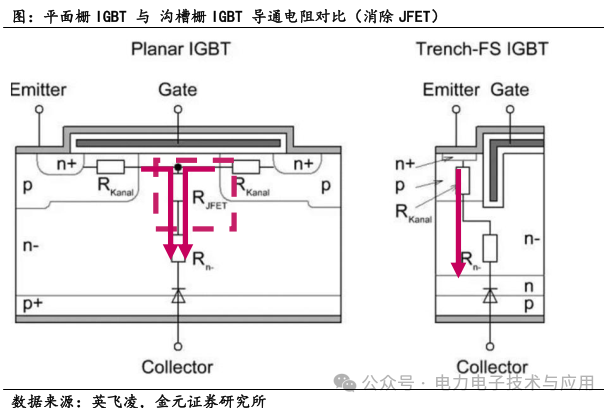
 • In 2023, the market size for IGBTs in China is approximately $2.8 billion, with a compound annual growth rate of about 12.1% from 2019 to 2023. According to Puyi’s forecast, the domestic IGBT market size is expected to reach approximately $3.1 billion in 2024, growing to $4.8 billion by 2029 (with a CAGR of 9.4%).
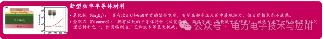
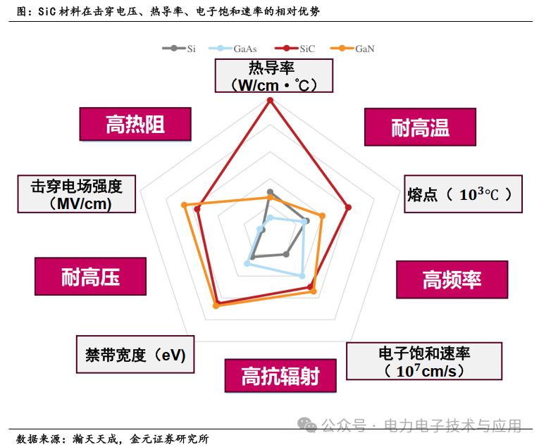
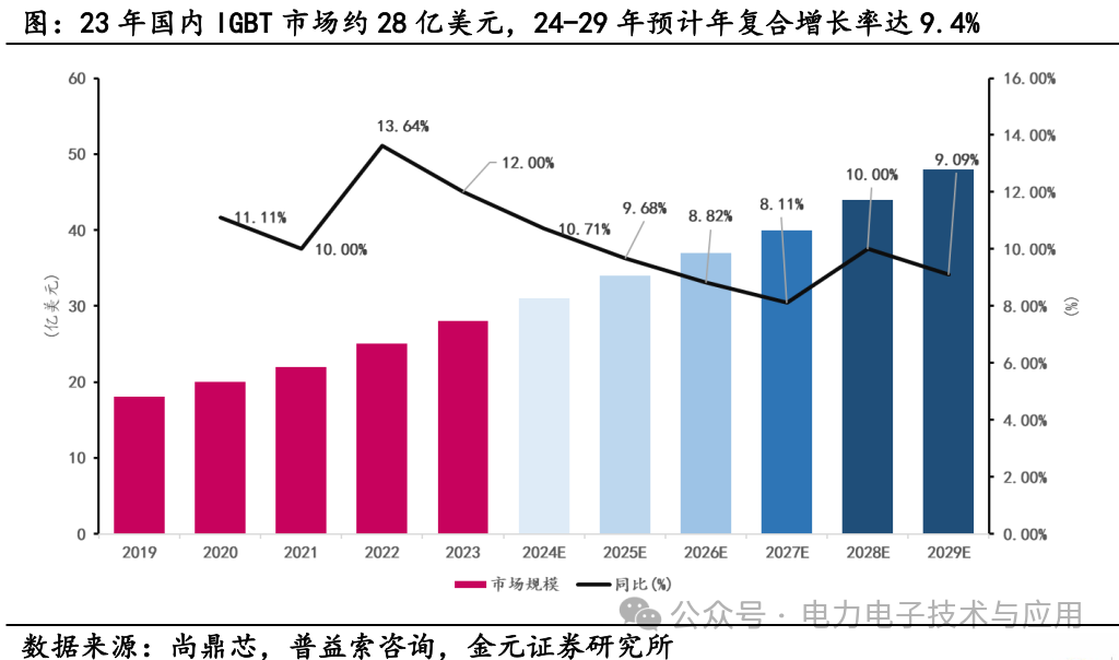 Wide Bandgap Semiconductor Materials Become Ideal Materials for High Voltage, High Power, and High Temperature• Silicon carbide (SiC) is a typical third-generation semiconductor material, offering significant advantages over silicon (Si) such as a larger bandgap, higher breakdown field strength, and thermal conductivity. The bandgap of SiC is approximately 3.26 eV (4HSiC, one of the polytypes), about three times that of silicon, resulting in an extremely low intrinsic carrier concentration, allowing devices to have low leakage at high temperatures and withstand higher electric fields without breakdown. Additionally, SiC’s critical breakdown field strength can reach about 3-4 MV/cm, approximately ten times that of silicon; its thermal conductivity is about 4.9 W/(cm·K), about three times that of silicon, which is beneficial for heat dissipation. These physical properties make SiC an ideal material for high voltage, high power, and high temperature electronic devices.
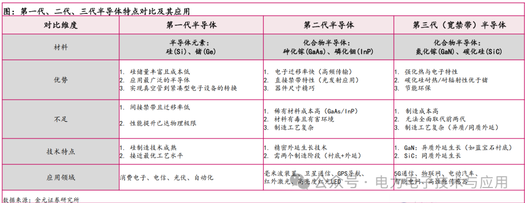 Overview of the Silicon Carbide Power Semiconductor Industry Chain
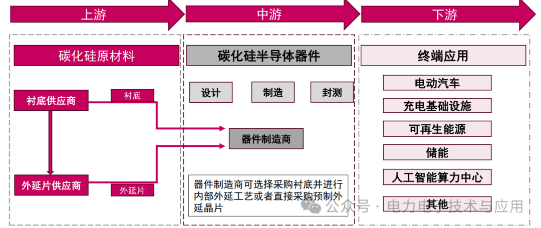 Silicon Carbide Gradually Penetrates AI + Smart Grid + eVTOL, Market Size Continues to Expand• The global market size for silicon carbide semiconductor devices is expected to reach approximately $2.6 billion in 2024, with a CAGR of 45.4% from 2020 to 2024; among which, the proportions for electric vehicles and charging infrastructure are high, at 74.4% and 7.8%, respectively. According to Yole forecasts, the silicon carbide device market is expected to reach $13.6 billion by 2029, driven by demand from emerging industries (including AI computing centers, smart grids, and eVTOL), with an expected CAGR of 56.4%, and the device penetration rate is projected to increase from 4.7% in 2024 to 17.1% by 2029.
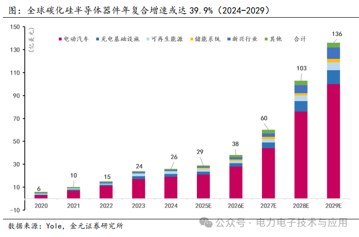
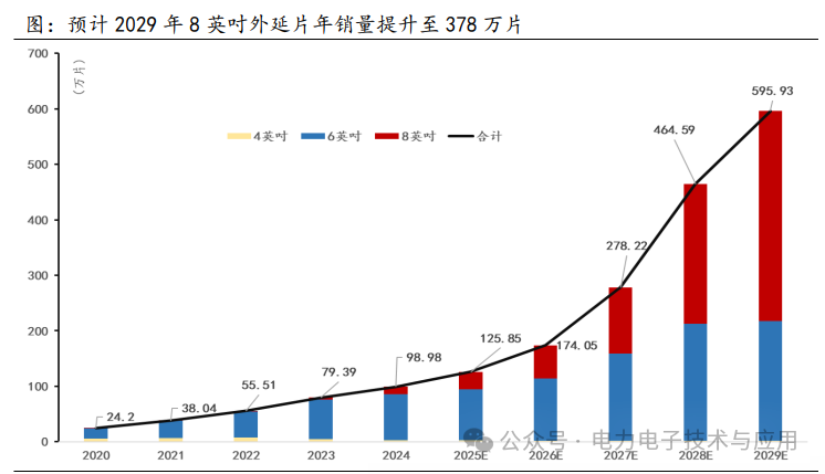
 Silicon Carbide Wafer Sizes Transition from 4-inch to 6-inch to 8-inch• The current mainstream SiC wafer size is 6 inches, with 8-inch wafers accelerating their penetration: from 2020 to 2024, the sales of 6-inch wafers are expected to grow from $300 million to $800 million, with a CAGR of 29.5%. The market size for 8-inch wafers is rapidly increasing, expected to reach $312 million in 2024, with a CAGR of 186.3% from 2020 to 2024. Considering the cost advantages of 8-inch wafers, it is expected that by 2029, the proportion of 8-inch SiC wafers will increase from 26% in 2024 to 77.4%, with the wafer market size reaching $5.8 billion.• In terms of sales, global silicon carbide wafer sales are expected to grow from 241,900 units in 2020 to 989,900 units in 2024, and further increase to 595,900 units by 2029. Among them, the sales of 6-inch wafers are expected to reach 822,800 units in 2024, while 8-inch wafer sales are expected to reach 137,100 units. As large-size technology matures further, it is expected that by 2029, 8-inch silicon carbide wafers will grow to 3,784,800 units, with a CAGR of 94.2%.
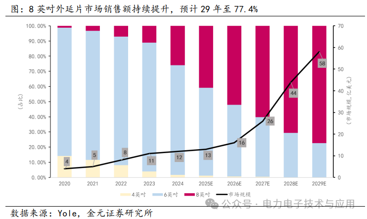
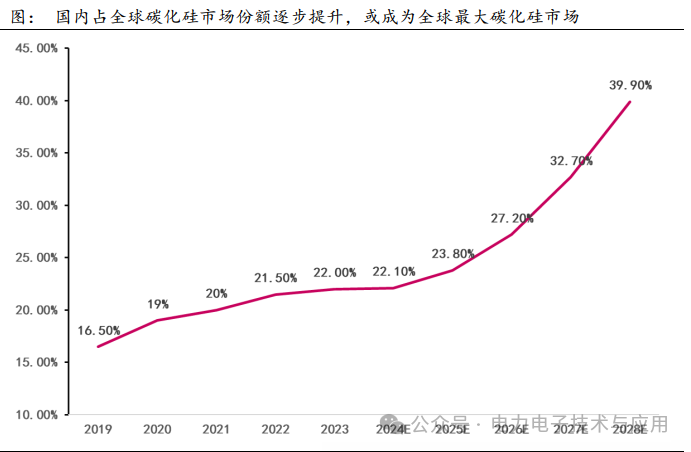
 China May Become the Top Market for Silicon Carbide• The growth of silicon carbide in the domestic market is particularly remarkable: benefiting from the rapid growth of applications in new energy vehicles, energy storage, and other power sectors, domestic 6-inch wafer sales are expected to grow from 34,000 units in 2019 to 188,000 units in 2023, with a CAGR of 52.8%, outpacing the global 6-inch sales growth of 46.1% during the same period.• Frost & Sullivan predicts that domestic 8-inch sales are expected to reach 1.03 million units by 2028, with a CAGR of 644.9% from 2023 to 2028. During the same period, global 8-inch silicon carbide sales are expected to reach 3.081 million units, with domestic demand for 8-inch wafers potentially accounting for 33.4% of the market share, and the overall demand for silicon carbide wafers accounting for about 40% of the global market share.
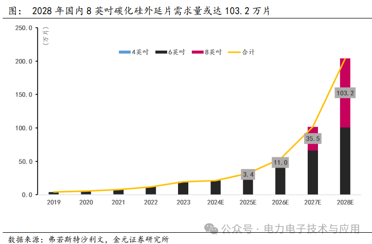
Performance Advantages of Silicon Carbide as a Power Semiconductor Material
• Silicon carbide power semiconductor devices stand out due to their excellent breakdown voltage, thermal conductivity, electron saturation rate, and radiation resistance. Compared to gallium nitride, silicon carbide has broader applicability in medium to high voltage applications, dominating the market above 600V, which is also larger in scale. In recent years, silicon carbide power semiconductor devices have been widely applied across multiple industries and are expected to play a key role in the ongoing transformation of the power semiconductor industry.
• In addition to traditional wafer processes, two important processes for silicon carbide power devices are the preparation of silicon carbide substrates and epitaxy.
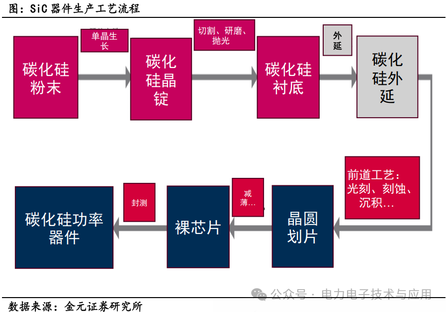
Preparation Process of SiC Substrates
• Silicon carbide single crystals are extremely rare in nature and can only be synthesized artificially. Currently, the industrial production of silicon carbide substrates primarily uses the PVT method. This method requires high temperature and vacuum to sublime the powder, and then controls the growth of components on the seed surface through thermal field control to obtain silicon carbide crystals. The entire process is completed in a closed space, with limited effective monitoring and many variables, requiring high precision in process control.
• Si + C = Silicon Carbide Powder: Si and C are synthesized in a 1:1 ratio to form SiC polycrystalline particles. SiC powder is the source for crystal growth, and its particle size and purity directly affect crystal quality, especially when preparing semi-insulating substrates, where the purity requirement is very high (impurity content <0.5ppm).
• Seed Layer: This is the foundation for crystal growth, providing the basic lattice structure for crystal growth and is the core raw material for crystal quality.
• Crystal Growth Physical Vapor Transport (PVT): The raw materials are heated, and the sublimated components are re-crystallized on the seed surface through vapor sublimation and thermal field control.
• Slicing: Diamond wire saws or laser cutters are used for slicing; SiC is a hard and brittle material, with hardness second only to diamond, thus slicing takes a long time and is prone to cracking.
• Grinding and Polishing: The substrate surface is processed to a nano-smooth mirror finish, which directly affects the surface roughness and thickness uniformity of Epi-ready substrates, subsequently impacting the quality of the epitaxy and, in turn, the quality of the devices.
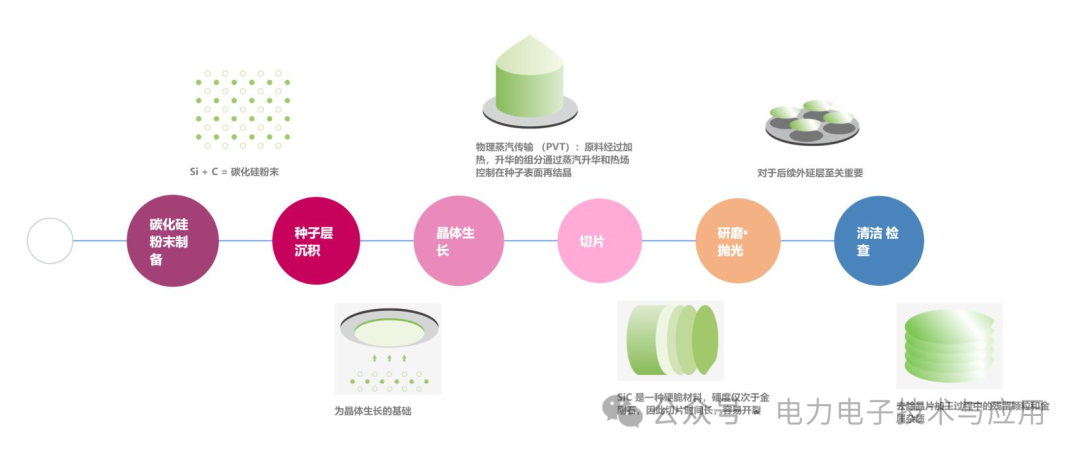
SiC Epitaxy Technology
• The epitaxial growth of silicon carbide (SiC) is mainly achieved through chemical vapor deposition (CVD) technology. Due to the lack of liquid phase characteristics of SiC, it is necessary to use silane (SiH₄) and propane (C₈H₃) or ethylene (C₂H₄) as precursors in the gas phase, with hydrogen or argon as the carrier gas, and deposition is performed at high temperatures (1500-1650°C).
• The process is divided into two steps: in-situ etching (using pure H₂ or mixed gases at about 1650°C to remove surface damage from the substrate and form a regular step structure) and main epitaxial growth (precisely controlling the thickness and uniformity of n-type or p-type doped layers). Defect management is a key challenge, requiring a combination of low-defect substrates and optimized processes to reduce the impact of lattice defects (such as dislocations and stacking faults) on device performance.
Source: Power Electronics Technology and Applications


【Disclaimer】The content of this public account is for reference only and does not constitute investment or business advice. Readers should verify the information and make cautious decisions. Some content is sourced from the internet; please contact us for handling if there is any infringement. The copyright of original content belongs to this public account, and reproduction or use without authorization is prohibited.
 Share
Share Collect
 View
View Like
Like