A common high-speed PCB design rule is to track the return current path of signals. In reality, this is much easier said than done, as the return paths for fast digital signals and even medium-frequency analog signals are largely confined beneath the traces. At very low frequencies or under direct current (DC), the return path can actually be anywhere, leading to some alternative wiring practices commonly seen in audio design, low-frequency sensor interface design, and pure DC systems. The ground layer only has advantages in terms of EMI shielding, but it does not directly confine the return path beneath the traces.
Some devices operate at low frequencies or DC, and these devices also form complete circuits, thus having a return path. Therefore, if you need to use one of these devices and assume that the signal-to-noise ratio (SNR) is low, how can you ensure that the return path loop does not become sensitive to noise?
Where is the DC Return Path?
I, along with many others, have drawn diagrams similar to the one below to illustrate the difference between the AC loop and the DC loop of the same trace. I won’t delve into the physical principles here, but it is well known that the AC loop is the path of least impedance, while the DC loop is the path of least resistance.
Now let’s consider how to maintain the DC return at the desired level in specific situations. Clearly, the DC return path can be located anywhere, including beneath the input traces (assuming a single-ended interface). This fact, along with the conductor interfaces with components, determines how to limit the DC return path and how to achieve low noise at low frequencies. To understand how this applies to various analog components or sensors, let’s look at some examples.
Sensors with Differential Interfaces
Differential interfaces are not only applicable to differential pairs that transmit high-speed signals. Low-frequency or analog interfaces can also be differential. In this case, the reading of low-frequency or DC signals is the same: the signal voltage is viewed as a potential difference between two conductors. Examples of these components include:
- RTD sensors
- Pressure sensors
- Outputs of differential amplifiers
- Position sensors
A similar idea applies to integration, where a DAC or adjustable DC power supply is used to generate a voltage, which is then amplified/driven through a differential output. In either case, the factors determining the noise received on that DC interconnect are the same.
This can be considered the simplest of the three cases introduced in this article. The reason is simple: you are wiring a differential pair, which should be routed through the ground plane. Under DC conditions, this differential pair completely confines the return current to the negative side of the interface. Since there are no switches, there is no displacement current in the nearby ground plane, so we do not need to worry about tracking this portion of the return current. Aside from length adjustments, standard differential pair routing rules apply here.
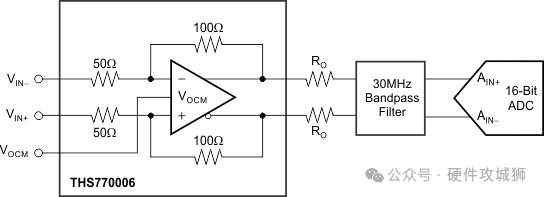
Differential amplifiers and differential ADC interfaces. For DC signals, each trace provides a complementary return path for the other trace. This diagram shows Texas Instruments’ THS770006, but other differential components can also be used for DC sensor interfaces.
Two-Wire Sensor Interfaces with Common Ground
One example I encountered recently in a precision motion control project involved a pair of wires transmitting out-of-phase sine waveforms. The analog front end measures the phase difference between these two wires and uses a reference oscillator signal to extract the phase difference, thereby determining the position of a small motor very accurately.
In this case, you do not have a true differential interface, as you have two independent wires sharing a common ground. The common ground carries the return current, while each wire carries a portion of the signal. When the signal-to-noise ratio (SNR) is low, the area with the return current should be isolated from all other ground areas. One method is to set up smaller ground discontinuities around the sensor interface.
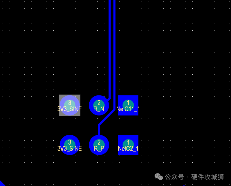
This two-wire interface provides a simple way to control noise without a true differential pair.
In some cases, another option is to connect multiple sets of differential DC lines to the analog front end. In the diagram below, I show the input from a D-Sub connector from a motor rotary transformer. The left and right differential pairs are detected separately, and their difference is used to determine the motor position. Since there is a return path in the corresponding lines, there is no need for ground cuts.
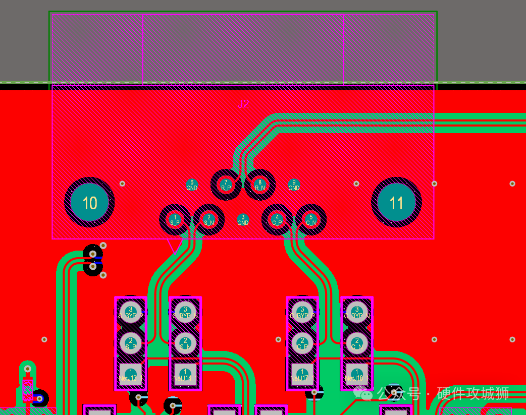
By cutting away portions of the copper in the ground layer, you can control where the DC return may exist. The limitation here is that you cannot route in the split areas of any other layers. If any traces carrying signals cross the cutout area, radiation issues will arise. A simple method is to define a no-go zone that overlaps all layers, ensuring that no copper is placed in the area surrounding the two-wire interface.
Interfaces with Common Power and Ground
In this type of interface, power and ground are shared between the PCB and external devices. There are two scenarios:
- The external device provides power and signals to your PCB
- Your PCB provides power to the external device, and the device provides signals to the PCB
The first scenario is easier to manage, as the power return point is directly connected to the external device. When the signal and power share the connector, this scenario is easiest to manage, as it forces the DC return path to be in the same location as the DC/low-frequency signals. The return current of low-level signals is confined within the cable/connector, keeping it away from any other signals that may cause crosstalk.
The second scenario is more common and more complex; the complete circuit loop will extend to the power regulator of the DC interface. Therefore, the return path can be very unpredictable, which may require placing the power supply closer to the sensor interface. If this can be achieved, a region can be created in the design that contains only the required DC/low-frequency signals, and that region can maintain good noise immunity.
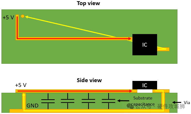
These small ultrasonic sensor boards draw power from the host PCB and transmit signals through the same interface. This may provide opportunities for your signals to pick up noise.
— End —
Disclaimer: This account maintains neutrality regarding all original and reprinted articles’ statements and viewpoints. The articles are provided for readers’ learning and communication purposes. Copyright for the articles, images, etc., belongs to the original authors. If there is any infringement, please contact for removal.
Recommended Reading:Why do we often require MOSFETs to turn off quickly but not to turn on quickly?High-Speed Interface Layout GuidelinesBuying an Oscilloscope for 3 Million: A Look Inside! (I was truly enlightened)