
 Introduction
This article uses a synchronous step-down converter power IC in an SOP-8 package as an example to introduce the PCB design for power supplies.

Related Parameters
As mentioned in “Guidelines for PCB Design of DC/DC Switching Power Supplies: Part One”, it is essential to understand the related parameters before starting the design, as shown in Figure 1:
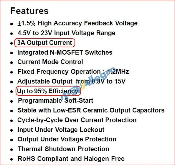
Figure 1

Pin View
The pin view provides an overview of the positions of the input/output pins, feedback, and other signal pins, as shown in Figure 2:
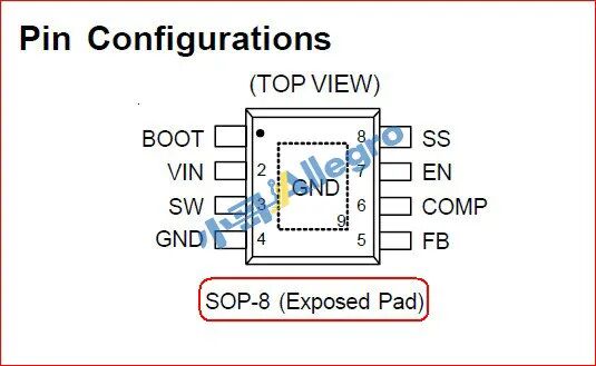
Figure 2
Official Recommended Circuit Diagram
The official recommended circuit diagram is shown in Figure 3:
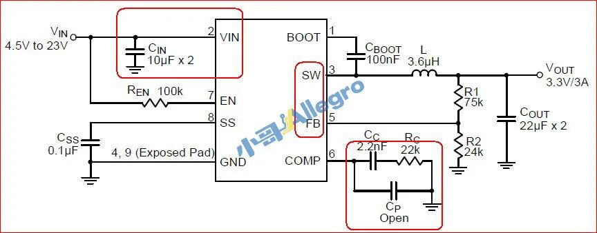 Figure 3
Pin 2 (VIN) is the input pin;
Pin 3 is the output pin;
Pin 5 is the feedback pin;
Pin 6 is the compensation pin.
Recommended Design Method
The recommended design method is shown in Figure 4:
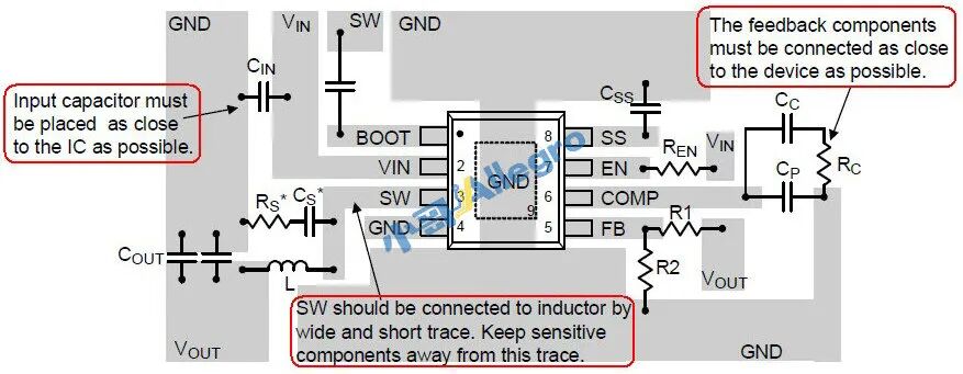
Figure 4
Design of SOP-8 Package Power IC
The following is the actual PCB design of this SOP-8 package power IC, as shown in Figure 5:
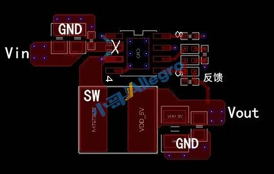
Figure 5
In Figure 5, the copper width at point “X” should not exceed the width of the pad for the pins;
Optimizing Layout
This diagram shows that the feedback, input/output current-carrying paths, and SW are handled to meet basic requirements. However, the input/output loop area is relatively large, and the layout can be optimized for a more balanced and aesthetically pleasing design with a smaller loop area. Additionally, pay attention to ground handling, as shown in Figure 6:
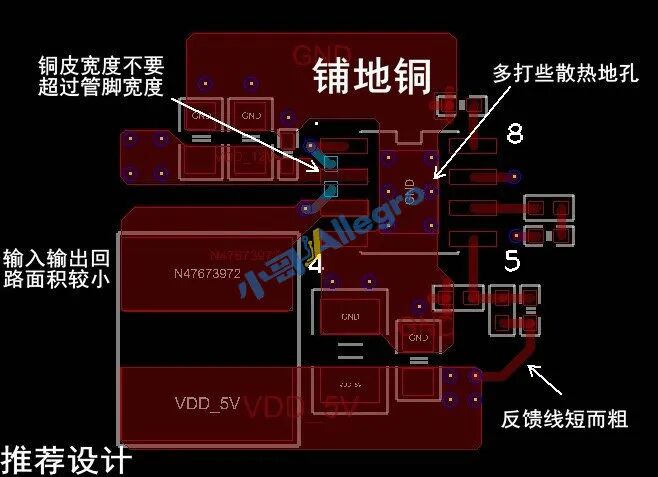
Figure 6
Loop Schematic
The schematic of the input/output loop when the power IC is conducting is shown in Figure 7:
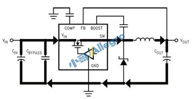
Figure 7
 Conclusion
As mentioned in “Guidelines for DC/DC Power Design: Part One”, attention must be paid to the following in switching power supply design:
1. The input capacitor (Cin) should be placed as close as possible to pin 2;
2. Use short and wide copper traces to connect the inductor and pin 3, and avoid long distances (SW should be connected to the inductor by wide and short trace. Keep sensitive components away from this trace.);
3. The feed line at pin 5 should be short, with a width of 15-20 mils, and the feedback line should be kept away from inductors, diodes, etc. (The feedback components must be connected as close to the device as possible.);
4. The output capacitors (Vout) should be arranged in descending order of capacitance, and the same applies to the input capacitors;
5. Components at pin 6 should be placed nearby;
6. The pad at pin 9 is a thermal pad, and it is recommended to have openings on both the top and bottom, with some ground holes placed on the pad;
7. The input/output loop area should be minimized;
8. No other traces should run under the IC;
9. Consider the current-carrying capacity of the input/output;
10. There should be no other signal copper or traces near the inductor area;
11. The trace width should not exceed the width of the pad for the pins;
The above is a design example of a synchronous step-down converter in an SOP-8 package, and the considerations mentioned are also applicable to other switching power supplies.
Disclaimer:“Original article, sharing is welcome, but unauthorized reproduction is strictly prohibited!”